

Silicon slice with asymmetry edge contour and manufacturing method thereof
An edge profile and asymmetrical technology, applied in semiconductor/solid-state device manufacturing, semiconductor/solid-state device parts, semiconductor devices, etc., can solve the problems of reduced process pass rate, particle pollution, induced process defects, etc., to reduce particle pollution , The effect of improving the qualification rate of the process
- Summary
- Abstract
- Description
- Claims
- Application Information
AI Technical Summary
Problems solved by technology
Method used
Image

Examples
Embodiment Construction
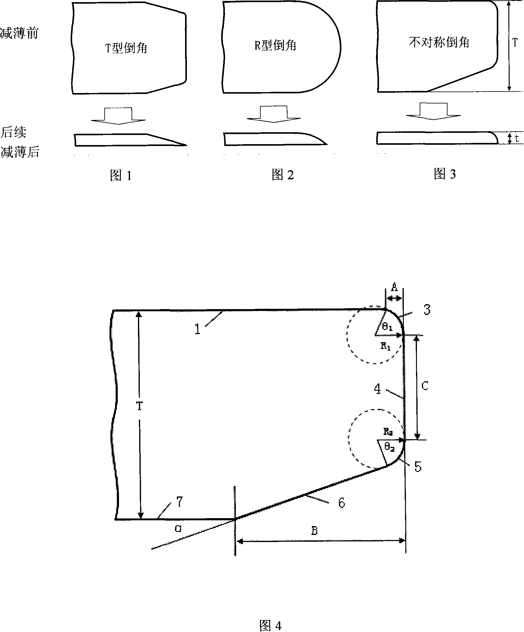
[0022] A preferred embodiment of the present invention is described as follows with reference to the accompanying drawings: Referring to FIG. 4 , the silicon wafer with an asymmetrical edge profile of the present invention has an asymmetrical shape consisting of arcs and straight lines. The upper surface 1, the lower surface 7, and the tip face 4 of the silicon wafer are linear parts, the upper surface 1 is connected with the tip face 4 of the silicon wafer through the arc EP1 3, and the tip face 4 of the silicon wafer is connected through the arc EP2 5 and the hypotenuse 6 is connected to the lower surface 7 . The top end surface 4 of the silicon wafer is tangent to the arcs EP1 3 and EP2 5 , the arc EP1 3 is intersected with the upper surface 1 , and the arc EP2 5 is tangent to the hypotenuse 6 .
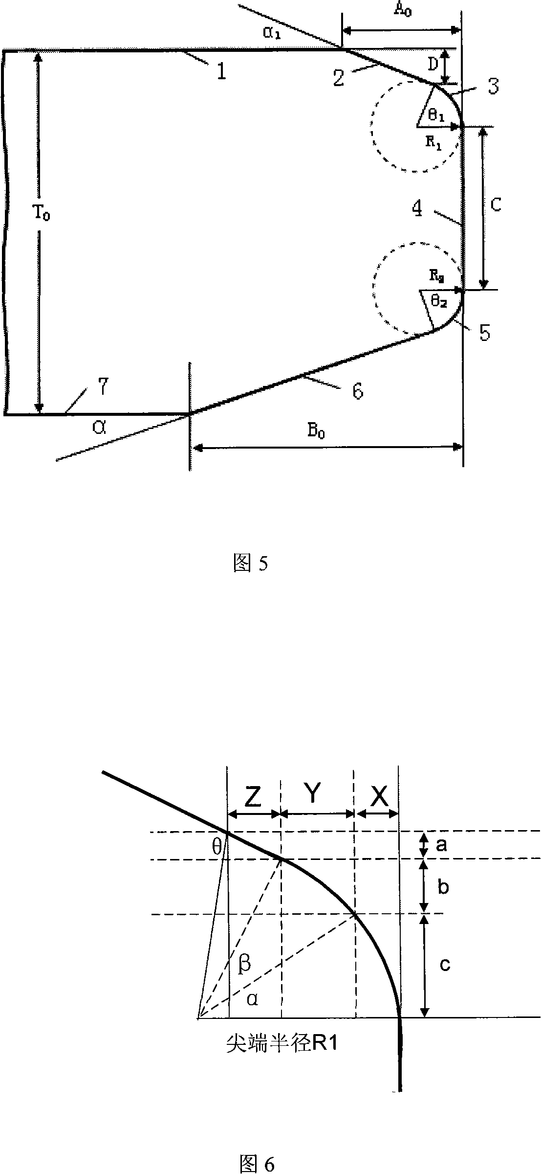
[0023] Referring to Fig. 4 and Fig. 5, the nouns represented by the symbols in the figures are: "T" represents the thickness of the semiconductor silicon wafer after polishing. "...
PUM
| Property | Measurement | Unit |
|---|---|---|
| Thickness | aaaaa | aaaaa |
Abstract
Description
Claims
Application Information