Semiconductor module, method for manufacturing the semiconductor module and portable device carrying the same
A manufacturing method and semiconductor technology, applied in semiconductor/solid-state device manufacturing, semiconductor devices, semiconductor/solid-state device components, etc., can solve the problems of reduced connection reliability, fewer places for resin discharge, and low fluidity of insulating layers, etc., to achieve Effect of improved connection reliability
- Summary
- Abstract
- Description
- Claims
- Application Information
AI Technical Summary
Problems solved by technology
Method used
Image

Examples
no. 1 approach
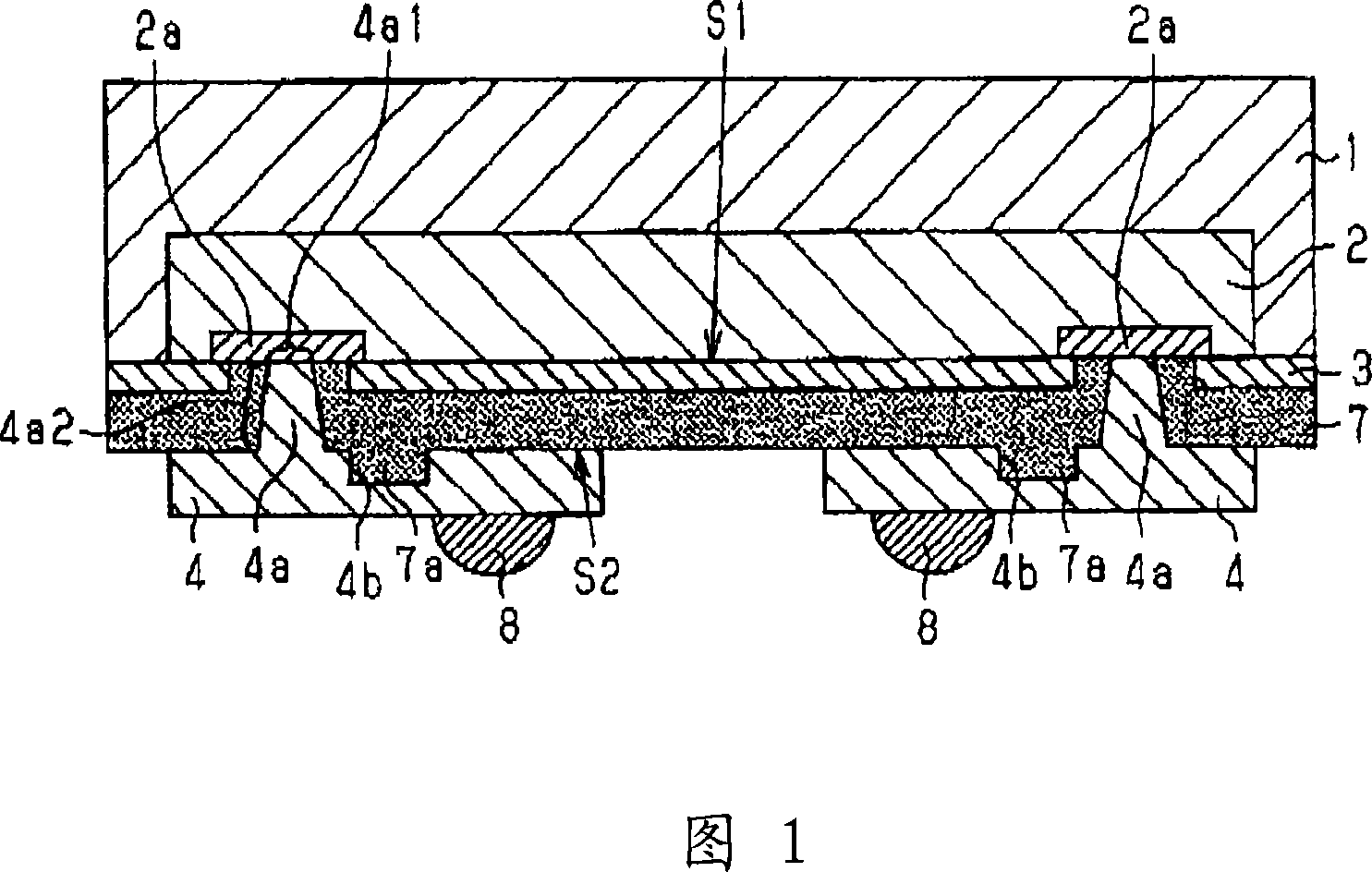
[0053] FIG. 1 is an outline sectional view of a semiconductor module according to a first embodiment of the present invention. A semiconductor module of a first embodiment is explained based on FIG. 1 .
[0054] The semiconductor substrate 1 adopts a P-type silicon substrate or the like, and circuit elements 2 such as predetermined circuits are formed on the surface S1 (lower side) by known techniques, and electrodes of the circuit elements 2 are formed on the surface S1 (especially the edge portion) that becomes the mounting surface. 2a. A protective film 3 is formed on a region on the surface of the semiconductor substrate 1 other than the electrode 2a. On the surface S1 (lower side) of the semiconductor substrate 1, an insulating layer 7 is formed on the electrode 2a and the protective film 3 in order to further expand the pitch of the electrode 2a, and the exposed surface of the electrode 2a is connected to the exposed surface of the electrode 2a through the insulating la...
no. 2 approach
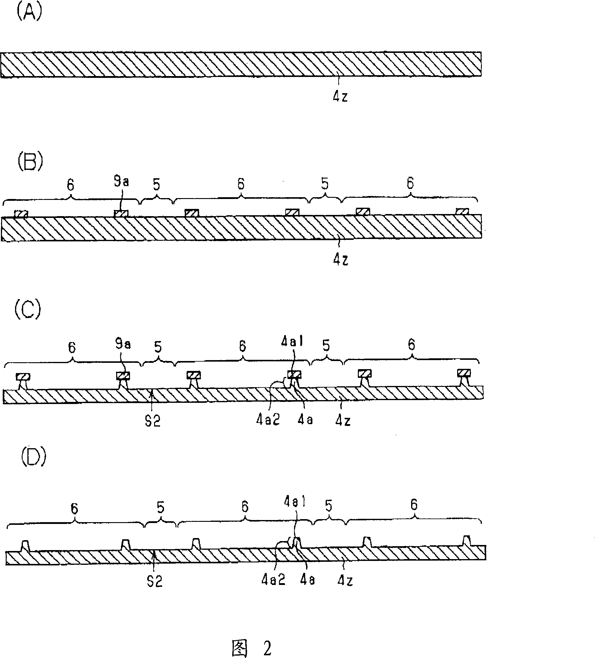
[0082] Fig. 7 is a cross-sectional view of a copper plate having protrusions and grooves for illustrating a second embodiment of the present invention. 8 and 9 are schematic cross-sectional views for explaining the manufacturing process of the semiconductor module of the second embodiment. Next, the manufacturing process of the semiconductor module of the second embodiment will be described with reference to FIGS. 7 to 9 .
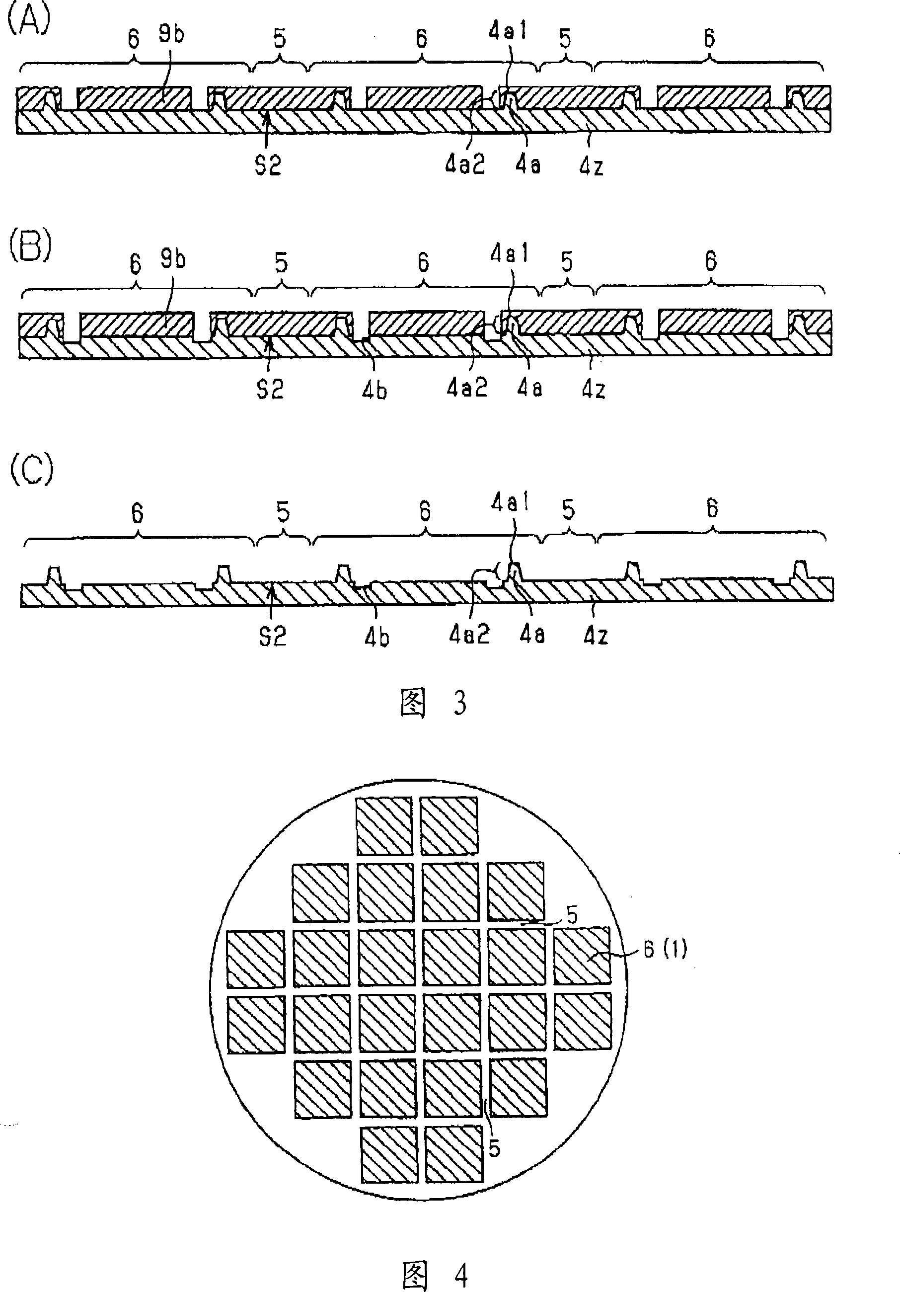
[0083] As shown in FIG. 7 , the difference from the copper plate having protrusions and grooves in the first embodiment is that grooves 4 b 1 are formed not in semiconductor module formation region 6 but in scribe lines 5 . In addition, the groove portion 4 b 1 is formed in a grid pattern so as to surround the semiconductor module formation region 6 (semiconductor substrate 1 ) along the scribe line 5 . The copper plate 4z having such a groove portion 4b1 can be easily produced by changing the mask pattern of the resist mask 9b shown in FIG. 3(A). Other ...
no. 3 approach
[0097] Fig. 10 is a cross-sectional view of a copper plate having protrusions and grooves for illustrating a third embodiment of the present invention. 11 and 12 are schematic cross-sectional views for explaining the manufacturing process of the semiconductor module of the third embodiment. Next, the manufacturing process of the semiconductor module of the third embodiment will be described with reference to FIGS. 10 to 12 .
[0098] As shown in FIG. 10, the difference from the copper plate having protrusions and grooves in the first embodiment is that the grooves 4b2 are formed corresponding to the spatial pattern of the rewiring pattern (wiring layer) 4. In addition, the depth of the groove portion 4b2 is the same as the height of the rewiring pattern (wiring layer) 4, which is about 30 µm. The copper plate 4z having such a groove portion 4b2 can be easily made by changing the mask pattern of the resist mask 9b shown in FIG. 3(A) and controlling the etching treatment condit...
PUM
 Abstract
Description
Claims
Application Information
 - R&D
- Intellectual Property
- Life Sciences
- Materials
- Tech Scout
- Unparalleled Data Quality
- Higher Quality Content
- 60% Fewer Hallucinations
Browse by: Latest US Patents, China's latest patents, Technical Efficacy Thesaurus, Application Domain, Technology Topic, Popular Technical Reports.
© 2025 PatSnap. All rights reserved.Legal|Privacy policy|Modern Slavery Act Transparency Statement|Sitemap|About US| Contact US: help@patsnap.com