Method for calibrating sub-nanometer critical dimension using pitch offset

A technology of key dimensions and calibration methods, applied in nanotechnology, components for opto-mechanical processing, measurement devices, etc., can solve the problems of damage to test wafers, poor calibration results, and high process costs

Active Publication Date: 2008-08-13
TAIWAN SEMICON MFG CO LTD
View PDF0 Cites 13 Cited by
  • Summary
  • Abstract
  • Description
  • Claims
  • Application Information

AI Technical Summary

Problems solved by technology

As such, these conventional test wafers do not align well below 1nm
In addition, the metrology step can damage the test wafer, requiring the manufacture and maintenance of several test wafers
It is possible to fabricate test wafers with sub-nanometer pitches, but the process is very expensive

Method used


Image

  • Method for calibrating sub-nanometer critical dimension using pitch offset
  • Method for calibrating sub-nanometer critical dimension using pitch offset
  • Method for calibrating sub-nanometer critical dimension using pitch offset

Examples


Embodiment Construction

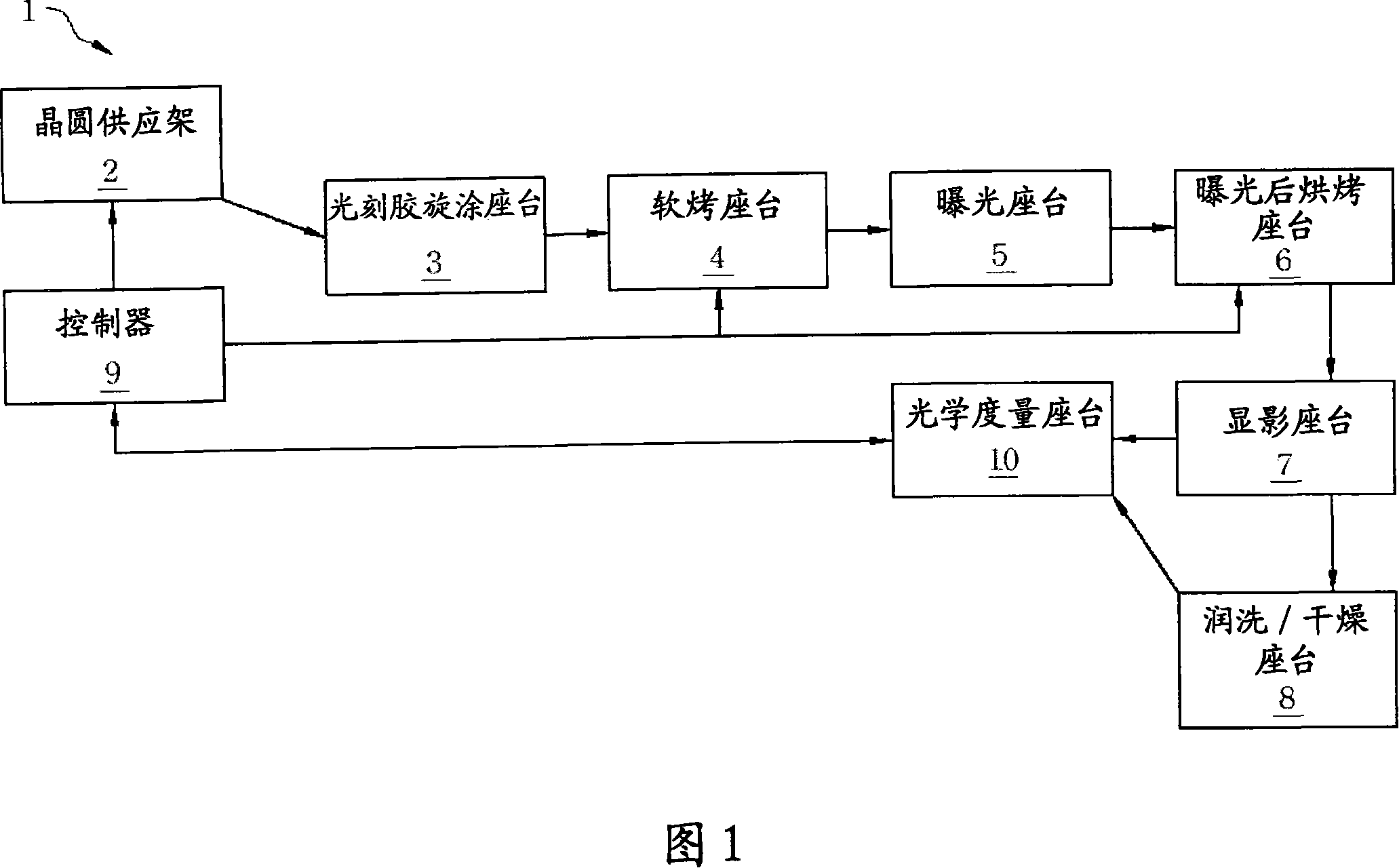
[0049] In order to further explain the technical means and effects of the present invention to achieve the intended purpose of the invention, the method for calibrating sub-nanometer critical dimensions proposed according to the present invention will be implemented in conjunction with the accompanying drawings and preferred embodiments below. Ways, methods, steps, features and effects thereof are described in detail below. For convenience of description, in the following embodiments, the same elements are denoted by the same numbers.

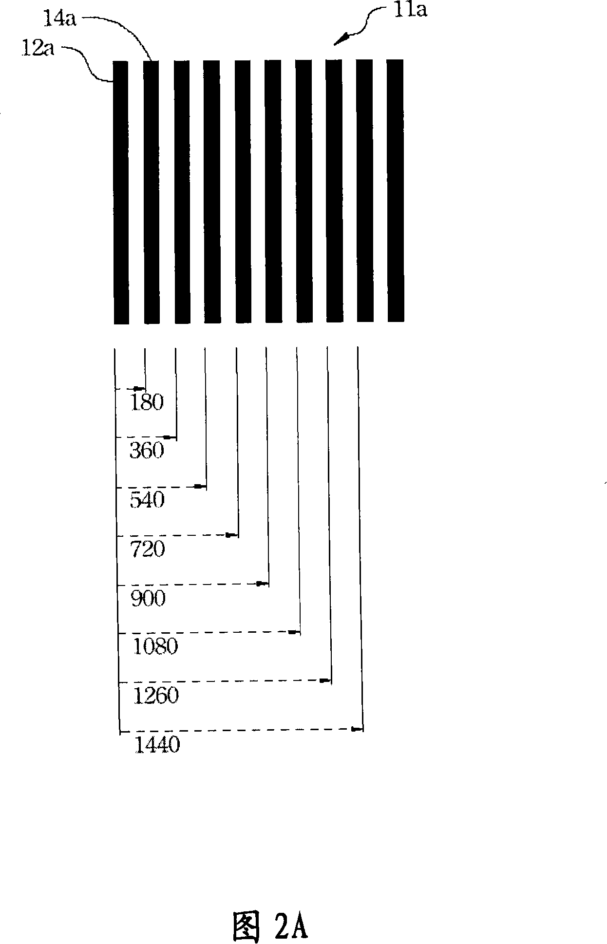
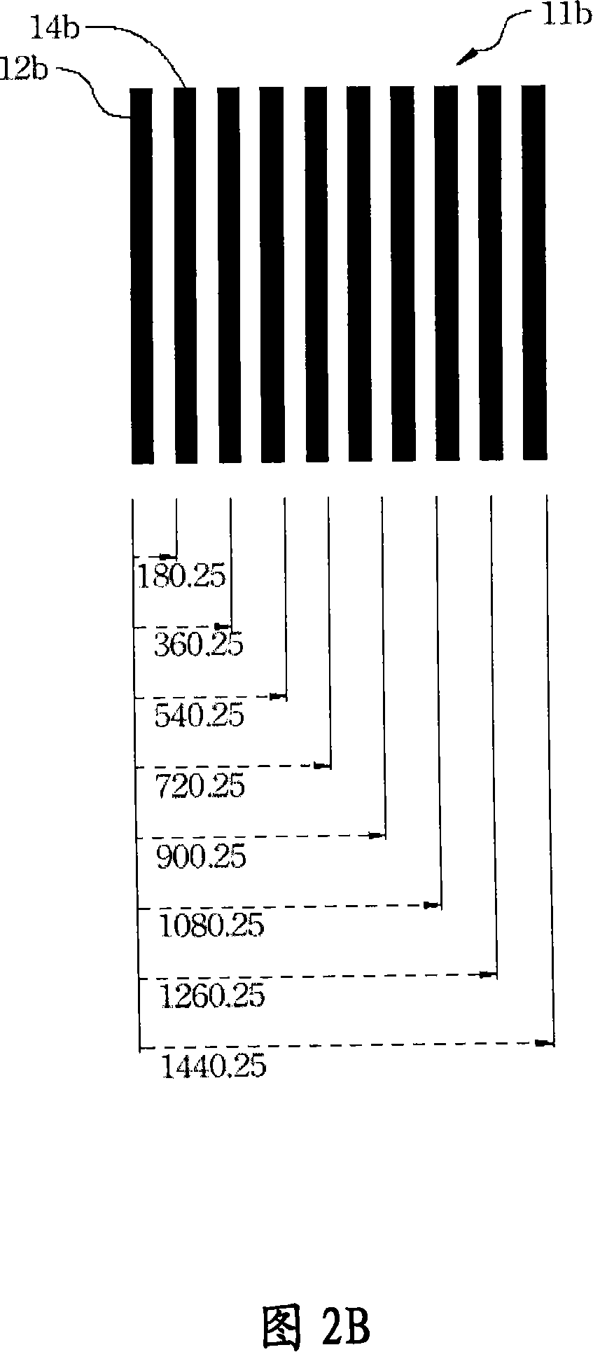
[0050] The present invention provides a method for calibrating a metrology tool or system. In an exemplary embodiment, a pattern layer is formed such that the formed shutter pattern has a known pitch plus an offset value, wherein the material of the pattern layer may include but not limited to photoresist, polysilicon, oxide, and the like. In an exemplary embodiment, the spacing value is less than 1 nanometer. The present invention facilitate...


PUM

PropertyMeasurementUnit
angle of incidenceaaaaaaaaaa

Abstract

The present invention relates to a method of calibrating sub-nanometer critical dimensions using pitch offsets, thereby calibrating metrology tools used to measure characteristics of semiconductor devices. A method for calibrating a sub-nanometer critical dimension using a pitch offset includes the steps of: measuring a first pitch; measuring a second pitch, wherein the second pitch is offset from the first pitch by a pitch offset; performing a comparison with the A step of comparing the first distance with the second distance; and judging the measurement accuracy according to the comparison step. From the aforementioned comparison, appropriate calibration steps can be taken to reduce the gap between the known and measured pitches. The method provided by the invention can effectively calibrate the metrology tool to the sub-nanometer level by using the offset of the sub-nanometer spacing.

Description

technical field [0001] The invention relates to a method for integrated circuit manufacturing process, in particular to a method for sub-nanoscale calibration of a measuring tool. In addition, the present invention can also be applied to photomask photomask process. Background technique [0002] In integrated circuit (integrated circuit; IC) manufacturing technology, generally a photoresist layer is coated on the surface of a semiconductor wafer first, and then the photoresist is exposed through a mask. Then, a post-exposure baking step is performed to change the physical properties of the photoresist to facilitate subsequent processing. Afterwards, an after development inspection (ADI) is performed to check the critical dimension of the photoresist by using a metrology system to determine whether it meets the specifications. If the photoresist is within specification, the pattern is etched or transferred and the photoresist is stripped. Then, after etching inspection (AE...

Claims


Application Information

Patent Timeline
Patent Type & Authority Applications(China)
IPC IPC(8): G03F7/20G03F1/14H01L21/66G01B11/02
CPCG03F7/70625G03F7/70516B82Y35/00G03F7/70608G03F7/70616H01L21/0274
Inventor 柯志明游信胜王育溪黄得智高蔡胜黄国骏
Owner TAIWAN SEMICON MFG CO LTD
Why Eureka
Try Eureka