Wafer with radiating structure and its production method
A technology of heat dissipation structure and manufacturing method, which is applied in semiconductor/solid-state device manufacturing, electrical components, electric solid-state devices, etc., can solve the problems of prolonged assembly time and increased assembly complexity, and achieve good heat dissipation effect
- Summary
- Abstract
- Description
- Claims
- Application Information
AI Technical Summary
Problems solved by technology
Method used
Image
Examples
Embodiment Construction
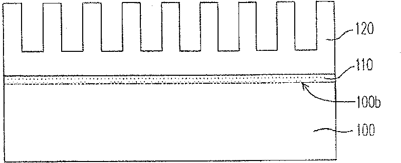
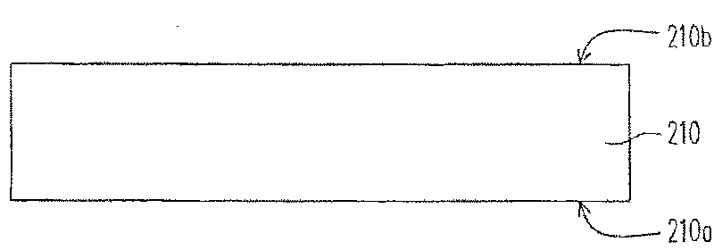
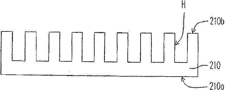
[0048] Figure 2A~2E Shown is a schematic cross-sectional view of a manufacturing process of a wafer with a heat dissipation structure according to an embodiment of the present invention. First, please refer to Figure 2A , A wafer 210 is provided. The wafer 210 has an active surface 210a and a back surface 210b opposite to the active surface 210a. After that, like Figure 2B As shown, a plurality of blind holes H are formed on the back surface 210b of the wafer 210. In this step, dry etching or wet etching can be used to etch the backside 210b of the wafer 210 to form these blind holes H. Since the shape of the blind hole H will affect the shape of the metal heat sink that is subsequently formed on the back 210b of the wafer 210, the user can design the blind hole H as a sheet or column according to their needs. Blind holes to form metal heat sinks in the form of fins or columns.
[0049] Next, please refer to Figure 2C As shown, a metal material is filled in the blind holes ...
PUM
 Abstract
Description
Claims
Application Information


