Optical waveguide containing Cu ion

A technology of optical waveguide and multi-mode optical waveguide, which is applied in the direction of optical waveguide and light guide, and can solve the problem of slow diffusion of Cu ions

Inactive Publication Date: 2008-08-27
ZHEJIANG UNIV
View PDF0 Cites 9 Cited by
  • Summary
  • Abstract
  • Description
  • Claims
  • Application Information

AI Technical Summary

Problems solved by technology

The disadvantage of this kind of optical waveguide is: because the salt containing Cu ions has a high melting point, on the other hand, the diffusion speed of Cu ions in the glass is very slow, and

Method used


Image

  • Optical waveguide containing Cu ion
  • Optical waveguide containing Cu ion

Examples


Embodiment Construction

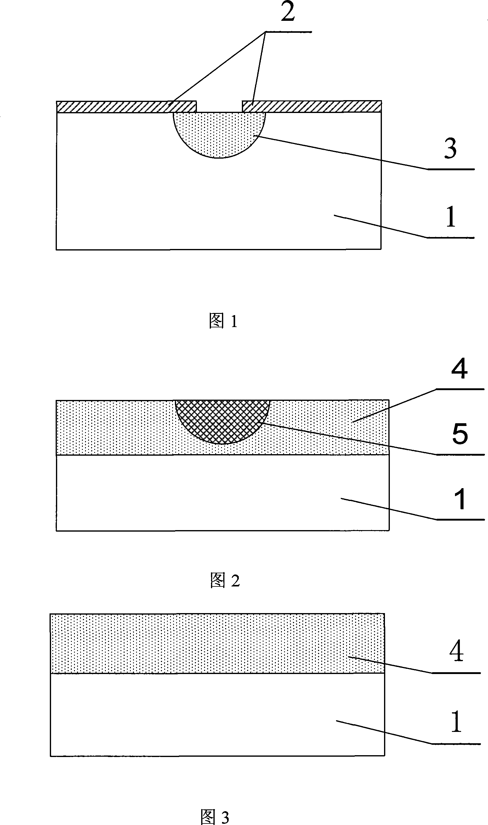
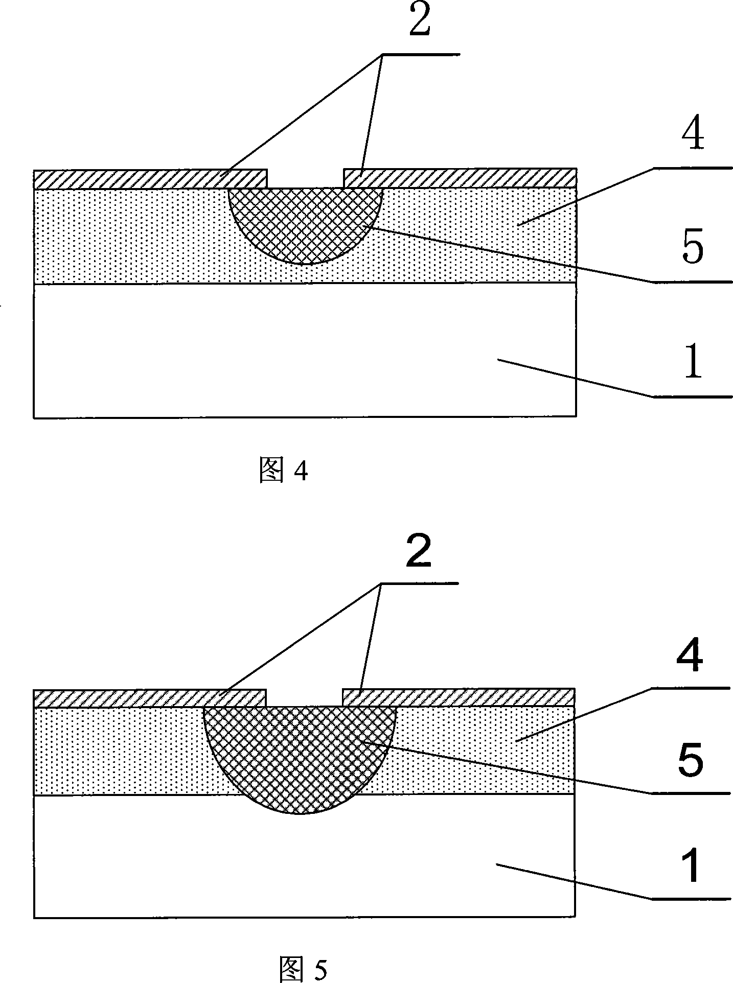
[0022] As shown in Fig. 2 and Fig. 4, the present invention is provided with planar Cu ion diffusion region 4 on the upper surface of glass substrate 1, is provided with strip-shaped high polarizability ion diffusion region 5 in planar Cu ion diffusion region 4, As the core layer of the optical waveguide, the refractive index of the strip-shaped high polarizability ion diffusion region 5 is higher than that of the glass substrate 1 and also higher than that of the plate-shaped Cu ion diffusion region 4 .

[0023] The material of the glass substrate 1 is silicate glass, borate glass or phosphate glass.

[0024] The high polarizability ion is Ag + , Tl + 、Cs + , Li + or Rb + ion.

[0025] The optical waveguide is a single-mode optical waveguide or a multi-mode optical waveguide.

[0026] The thickness of the strip-shaped high polarizability ion diffusion region 5 is smaller than the thickness of the flat Cu ion diffusion region 4 , or greater than the thickness of the flat...


PUM


Abstract

The invention discloses an optical waveguide with Cu ions. An upper surface of a glass substrate is provided with a flat shape Cu ion diffusion zone which is provided with a strip shape high polarizability ion diffusion zone which is used as a core layer of the optical waveguide and has a refractive index higher than that of the glass substrate and also higher than that of the flat shape Cu ion diffusion zone. Because the strip shape high polarizability ion diffusion zone is formed based on the flat shape Cu ion diffusion zone, an ion-exchange optical waveguide has a characteristic of blue-green luminescence of the Cu ions. Meanwhile, the optical waveguide avoids a process that an ion exchange of Cu and salt forms the ion exchange of strip shape optical waveguide under a high temperature condition in the manufacturing process, has a low requirement to a mask, thereby having a lower cost.

Description

technical field [0001] The invention relates to integrated optical device technology, in particular to an optical waveguide containing Cu ions. Background technique [0002] Integrated optical circuit means that on the surface of the same substrate, optical waveguides are made of materials with a slightly higher refractive index, and various optical devices such as light sources and gratings are made on this basis. Through this integration, the miniaturization, weight reduction, stabilization and high performance of the optical system can be achieved. With the development of modern optical fiber communication technology and optical fiber sensing technology, people pay more and more attention to integrated optical devices. [0003] The materials used for the production of integrated optical devices mainly include III-V semiconductor materials such as Si, silicon dioxide, gallium arsenide and indium phosphide, polymers, glass, etc. The glass optical waveguide device based on...

Claims


Application Information

Patent Timeline
IPC IPC(8): G02B6/10
Inventor 郝寅雷毛小丹杨建义江晓清周强李锡华王明华
Owner ZHEJIANG UNIV
Why Eureka
Try Eureka