High pressure resistant lateral direction bilateral diffusion MOS transistor

A MOS transistor, lateral double diffusion technology, applied in semiconductor devices, electrical components, circuits, etc., can solve problems such as unfavorable integration of other circuits, high cost, complex process, etc. Effect

Inactive Publication Date: 2008-09-03
PEKING UNIV
View PDF0 Cites 40 Cited by
  • Summary
  • Abstract
  • Description
  • Claims
  • Application Information

AI Technical Summary

Problems solved by technology

Usually, the core devices of this part of the circuit need to use special materials, the process is complicated, the cost is expensive, and it is not conducive to the integration with other circuits

Method used


Image

  • High pressure resistant lateral direction bilateral diffusion MOS transistor
  • High pressure resistant lateral direction bilateral diffusion MOS transistor
  • High pressure resistant lateral direction bilateral diffusion MOS transistor

Examples


Embodiment Construction

[0018] Below in conjunction with accompanying drawing and specific embodiment the present invention is described in further detail:

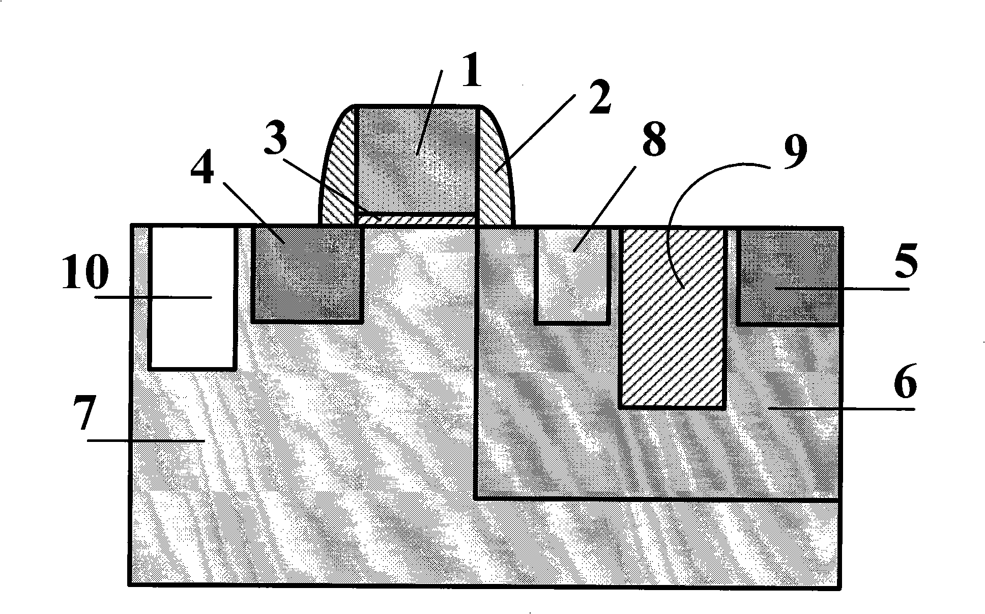
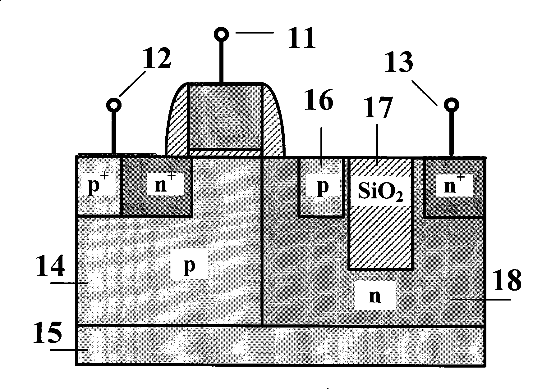
[0019] Figure 1 Knot The core part of the field effect transistor of the present invention is given in the structure. Most of its structure is the same as the conventional LDMOS structure, and its main special feature is that a doped region 8 with different doping types and an insulating dielectric region 9 are introduced into the low-doped drift region 6 . Usually, the doping concentration in the doped region 8 is higher than that in the drift region 6 . The insulating dielectric region 9 preferably uses an insulating material with a lower dielectric constant than silicon, such as silicon oxide, silicon nitride, and the like. Since the current of the device needs to flow in the drift region 6 , the depths of the doped region 8 and the insulating dielectric region 9 should not exceed the drift region 6 . The doped region 8 is flush with the ...


PUM


Abstract

The present invention discloses a transversal bilateral diffusion MOS transistor with high pressure resistant, which belongs to micro-electronics semi-conductor device field. The device includes a gate region, a source area, a drain region, a tagma, a gate medium and a drift region, the setting drift region is placed between the tagma and the drain region, and the doping type is opposite to the tagma, an insulating medium region and a doping region which is opposite to the doping type of the drift region are equipped in the drift region, and the doping concentration of the doping region is higher than that of the drift region, the doping region is adjacent to the tagma, however the insulating medium region is adjacent to the drain region. Because the insulating medium region and the doping region are inducted into the drift region at the same time, the effective depth of the drift region is reduced effectively to make the electric field more uniform and increase the equivalent length of the drift region, the resistant high Voltage characteristic of the transversal bilateral diffusion MOS transistor device of the present invention is good.

Description

technical field [0001] The invention relates to a lateral double-diffusion MOS transistor in the field of microelectronic semiconductor devices, in particular to a lateral double-diffusion MOS transistor suitable for a high-voltage circuit or a radio frequency power amplifier circuit. Background technique [0002] A lateral double-diffused MOS transistor (lateral double-diffused MOS transistor, LDMOS) is a lightly doped drain MOS device. Compared with ordinary MOS devices, LDMOS has a longer lightly doped region at the drain end, called the drift region, usually the doping concentration of this part of the structure is 10 16 cm -3 order of magnitude. The LDMOS structure bears a higher voltage drop through the drift region. Because LDMOS technology is simple, reliable, mature, and has good RF performance, and because the manufacturing process of LDMOS transistors is fully compatible with existing standard CMOS processes, it is easy to achieve large-scale integration with l...

Claims


Application Information

Patent Timeline
Patent Type & Authority Applications(China)
IPC IPC(8): H01L29/78H01L29/06
Inventor 肖韩黄如杨淮洲王鹏飞
Owner PEKING UNIV
Why Eureka
Try Eureka