Supercharge Your Innovation With Domain-Expert AI Agents!

LED element and luminous system and method for making LED element

A technology for light-emitting diodes and a manufacturing method, which is applied to electrical components, semiconductor devices, circuits, etc., can solve problems such as unfavorable luminous efficiency of light-emitting diode crystal grains, and achieve the effects of improving luminous efficiency and increasing luminous area.

Active Publication Date: 2008-09-03
BRIDGELUX INC
View PDF0 Cites 4 Cited by
  • Summary
  • Abstract
  • Description
  • Claims
  • Application Information

AI Technical Summary

Problems solved by technology

Therefore, the traditional wafer dicing techniques mentioned above are very detrimental to the luminous efficiency of LED dies with rectangular geometry today.

Method used


Image

  • LED element and luminous system and method for making LED element
  • LED element and luminous system and method for making LED element
  • LED element and luminous system and method for making LED element

Examples


Embodiment Construction

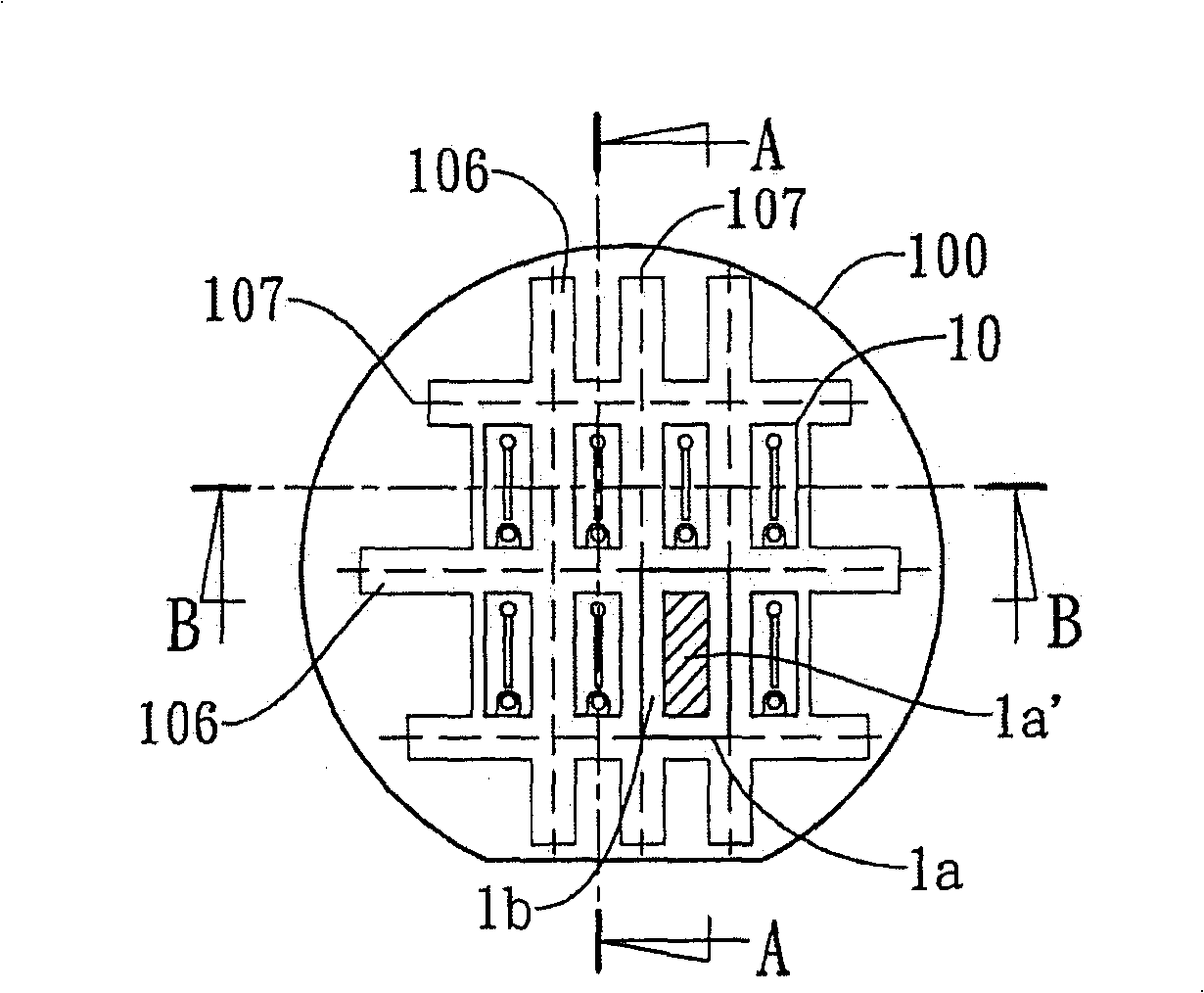
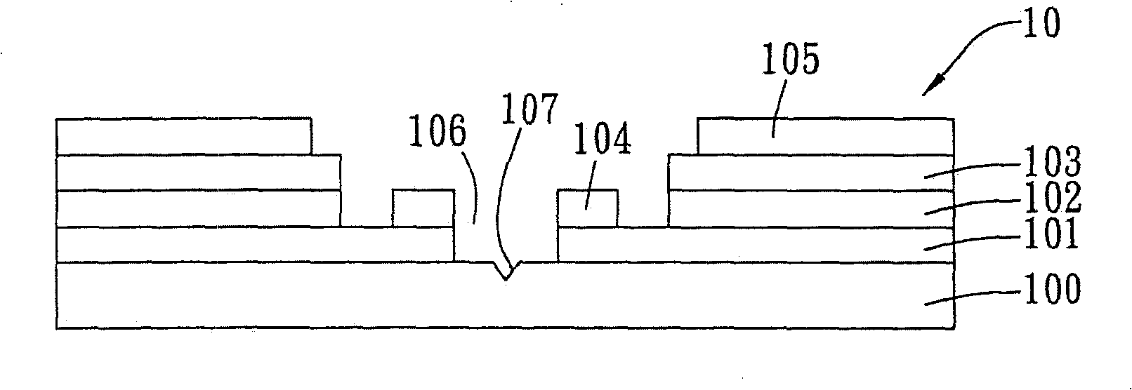
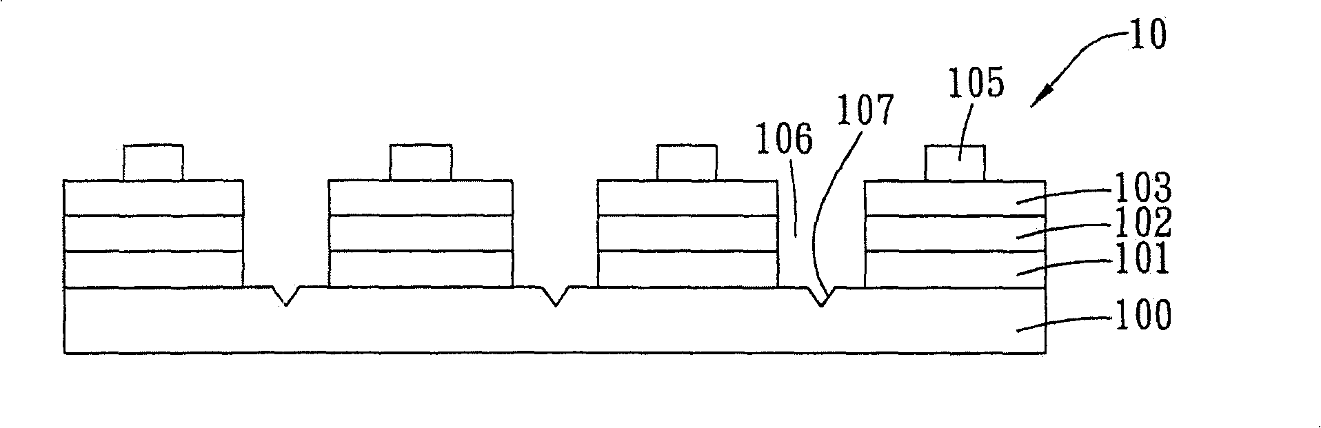
[0045] The present invention provides a self-aligned wafer dicing method (self-aligned wafersingulation method), which can separate LED chips on the wafer without pre-etching streets in at least one direction on the wafer. The method of the present invention can select at least one direction on the wafer without pre-etching the dicing line, for example, selecting the wafer at least along the crystal lattice direction that is most likely to break without pre-etching the dicing line, or on the two directions of the wafer without pre-etching the dicing line. eclipse cut. Since the wafer area is not occupied by the etching scribe along at least one direction, the wafer area occupied by each LED grain can be increased, thereby increasing its light-emitting area, so that the light-emitting efficiency of the LED element manufactured by the present invention is improved.

[0046] The light-emitting diode element and light-emitting system of the present invention and the method for man...


PUM

PropertyMeasurementUnit
Thicknessaaaaaaaaaa

Abstract

The present invention provides an element and a luminous system of a light-emitting diode and manufacturing method of the luminous diode element. The luminous diode element is produced by the self-aligned wafer singulation technique, in which the electric pole of each luminous diode grain is taken as the alignment mark forming the scribing lines on the chip, and a scribing street is not etched in advance between the adjacent luminous diode grains along at least one direction on the chip. Through the invention, the circumference area of the luminous diode grain is not occupied by the cutting path in at least one direction, the luminous area of the luminous diode grain can be increased to improve the light-emitting efficiency.

Description

technical field [0001] The present invention relates to a light-emitting diode element, a light-emitting system and a method for manufacturing the light-emitting diode element; in particular, it relates to a light-emitting diode element manufactured by self-aligned wafer cutting technology. Background technique [0002] The traditional manufacturing method of light-emitting diode devices grows epitaxial layers such as gallium indium aluminum nitride (Al InGaN) on sapphire or silicon carbide (SiC) wafers, and the gallium indium aluminum nitride epitaxial layers include at least N-type and P-type The epitaxial layer and the light-emitting layer in between, the wafer is processed to provide ohmic contacts (ohmic contacts) to the N-type and P-type epitaxial layers respectively, and then wafer dicing technology is used to separate the LED die from the wafer . Figure 1A It is a schematic top view of traditional light-emitting diode grains grown on a wafer, Figure 1B for along ...

Claims


Application Information

Patent Timeline
IPC IPC(8): H01L33/00H01L33/20
Inventor 刘恒莫庆伟
Owner BRIDGELUX INC
Features
  • R&D
  • Intellectual Property
  • Life Sciences
  • Materials
  • Tech Scout
  • Unparalleled Data Quality
  • Higher Quality Content
  • 60% Fewer Hallucinations
Learn More