A pixel driving circuit in silicon base organic luminescent display device

A pixel driving circuit and light-emitting display technology, which is applied in the fields of logic circuit coupling/interface, logic circuit connection/interface arrangement, electrical components, etc. using field effect transistors, which can solve difficult grayscale display, influence, and current inconsistency of organic light-emitting diodes. Stability and other issues, to achieve the effect of improving aperture ratio, uniform display, and reducing power consumption

Inactive Publication Date: 2008-09-10
SHANGHAI UNIV
View PDF0 Cites 27 Cited by
  • Summary
  • Abstract
  • Description
  • Claims
  • Application Information

AI Technical Summary

Problems solved by technology

[0009] However, it is very difficult for conventional voltage-driven pixel circuits to achieve high-level grayscale display. This is due to issues such as process manufacturing, even between different pixels on the same substrate, the threshold voltage V between transistors of the same type TH There will also be changes, causing the current flowing through the organic light-emitting diode to vary greatly with different pixels, making the current through the organic light-emitting diode unstable, and it is difficult to control the grayscale display
Process manufacturing will also bring inconsistencies in carrier mobility, which will further affect the uneven brightness of display pixels

Method used


Image

  • A pixel driving circuit in silicon base organic luminescent display device
  • A pixel driving circuit in silicon base organic luminescent display device
  • A pixel driving circuit in silicon base organic luminescent display device

Examples


Embodiment Construction

[0029] A preferred embodiment of the present invention is described as follows in conjunction with accompanying drawing:

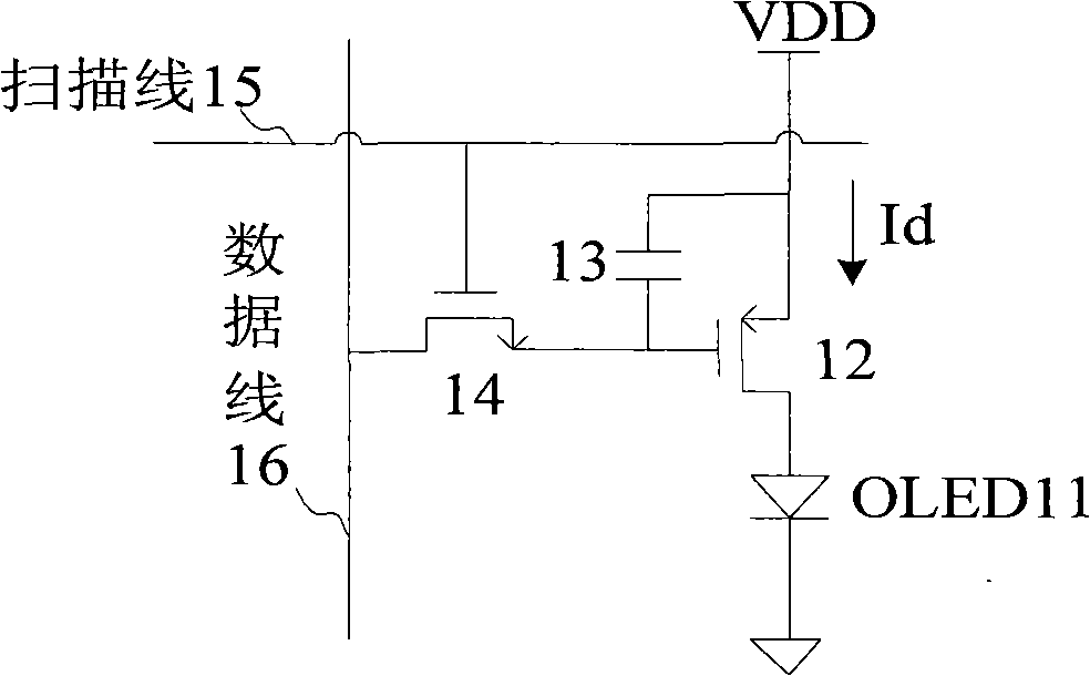
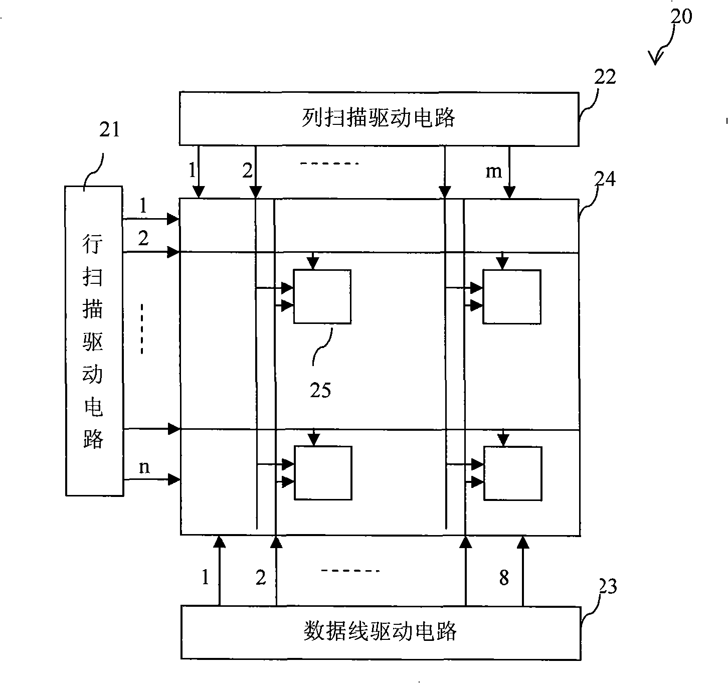
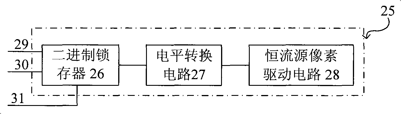
[0030] refer to figure 2 , figure 2 It is a schematic diagram of a silicon-based organic light-emitting display device 20 using the present invention, which includes a row scanning driving circuit 21 , a column scanning driving circuit 22 , a data line driving circuit 23 , and a display panel 24 . The pixel driving circuits 25 are arranged in a matrix on the display panel 24 to form a display device. figure 2 Among them, the row scanning driving circuit 21 sequentially scans and drives the row scanning lines 1 to n, and each row scanning line is electrically connected to an input terminal of the pixel driving circuit 25 corresponding to the row. The column scanning driving circuit 22 sequentially drives the column scanning lines 1 to m, and each column scanning line is electrically connected to another input end of the corresponding pixel driving circ...


PUM


Abstract

The invention relates to a pixel driving circuit in a silica-based organic luminous display, which is a pixel driving circuit that an input electricity is connected with a column scan line, a row scan line and a data line while an output electricity is connected with a diode, wherein the pixel driving circuit is connected with a pixel driving circuit with a constant current source through a level shifter circuit by a binary latch; the binary latch is used for gate of column and row data of the display equipment; the pixel driving circuit with the constant current source is used for providing current with fixed amplitude for an organic light emitting diode under pixel gate condition to allow organic light emitting diode to light, and change the intensity according to duty ratio of data provided by the data line; the level shifter circuit is used for high and low level shifting between the binary latch and the pixel driving circuit with the constant current source; the pixel driving circuit transmits data on a data line to the pixel driving circuit according to a column scan line and a row scan line, which results in gray-scale display of the organic light emitting diode. The whole pixel driving circuit of the invention adopts a transistor for charge and discharge instead of a traditional capacitor, thus the aperture ratio of the pixel circuit is significantly improved; through the constant current provided by a quiescent current source, the current passing under operating condition of the organic light emitting diode can be accurately controlled and not influenced by a threshold voltage.

Description

technical field [0001] The present invention relates to a pixel drive circuit (Pixel Circuit) in a silicon-based organic light-emitting display device (OLED-on-Silicon), in particular to a constant current source pixel connected by a binary latch through a level conversion circuit. A pixel driving circuit composed of a driving circuit. Background technique [0002] Silicon-based organic light-emitting display devices use organic light-emitting diodes as light-emitting devices, and use complementary metal oxide semiconductors as switching components or driving components of organic light-emitting diodes, including active pixel drivers, row scanning driving circuits, and column scanning drivers. circuit and the necessary control circuit, the purpose is to minimize the total number of chips and reduce the cost of the system. [0003] Compared with liquid crystal display devices (Liquid Crystal Display, LCD), organic light-emitting diodes have all-solid-state, simple process, l...

Claims


Application Information

Patent Timeline
IPC IPC(8): G09G3/32H03K3/356H03K19/0185G09G3/3225
CPCG09G3/3233G09G2320/064G09G2300/0871G09G2300/0857
Inventor 冉峰杨云霞徐美华程东方沈伟星陈章进姚树建康希
Owner SHANGHAI UNIV
Why Eureka
Try Eureka