Novel anti-reflection conductive film
An anti-reflection and conductive film technology, applied in optics, instruments, optical components, etc., can solve the problems of low yield, complex process, high cost, etc., achieve the effect of small thickness, simplified process, and continuous batch production
- Summary
- Abstract
- Description
- Claims
- Application Information
AI Technical Summary
Problems solved by technology
Method used
Image

Examples
Embodiment 1
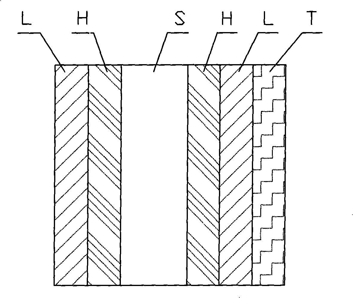
[0040] Embodiment 1: L / H / S / H / L / T type anti-reflection conductive film of the present invention
[0041] The specific film features of the L / H / S / H / L / T type anti-reflection conductive film of the present invention are:
[0042] The high refractive index layer (H) uses TiO 2 , the refractive index index of the material at 530-570nm is 2.1-2.4;
[0043] The low refractive index layer (L) is made of SiO 2 , the refractive index of the material at 530-570nm is 1.4-1.5;
[0044] The substrate material (S) is selected from glass, and the refractive index in the visible range is 1.51-1.56;
[0045] The transparent conductive film (T) is made of ITO, and the refractive index in the visible light range is between 1.85-1.95;
[0046] The thickness of each layer is designed as follows:
[0047]
[0048] refer to figure 1 , the reflection color of this film layer is light blue, and the reflectance value at the wavelength of 530nm-570nm can reduce the reflectivity of the original su...
Embodiment 2
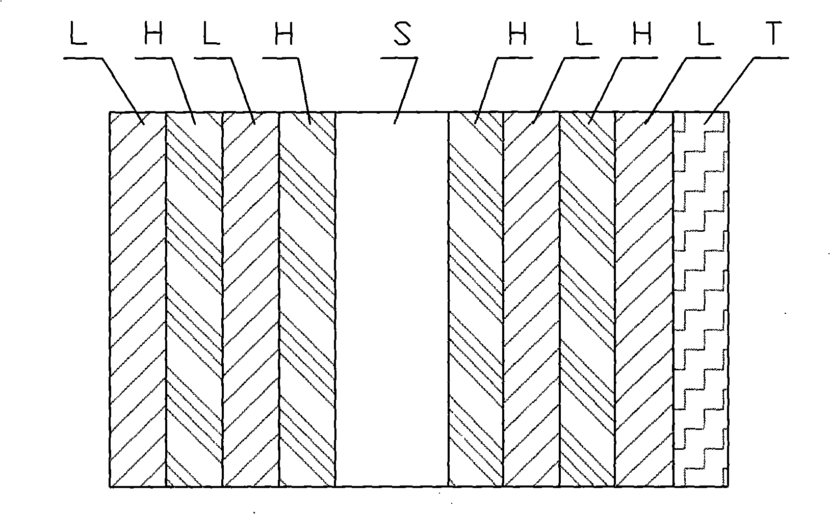
[0056] Embodiment 2: (L / H) of the present invention 2 / S / (H / L) 2 / T type anti-reflection conductive film
[0057] (L / H) of the present invention 2 / S / (H / L) 2 The / T type anti-reflection conductive film has a 9-layer structure with a large number of layers, but this structure can realize a variety of colors, so that the required color can be adjusted according to the needs. The specific film layer features are:
[0058] The high refractive index layer (H) uses TiO 2 , the refractive index index of the material at 530-570nm is 2.1-2.4;
[0059] The low refractive index layer (L) is made of SiO 2 , the refractive index of the material at 530-570nm is 1.4-1.5;
[0060] The substrate material (S) is selected from glass, and the refractive index in the visible range is 1.51-1.56;
[0061] The transparent conductive film (T) is made of ITO, and the refractive index in the visible light range is between 1.85-1.95;
[0062] The thickness of each layer is designed as follows:
...
Embodiment 3
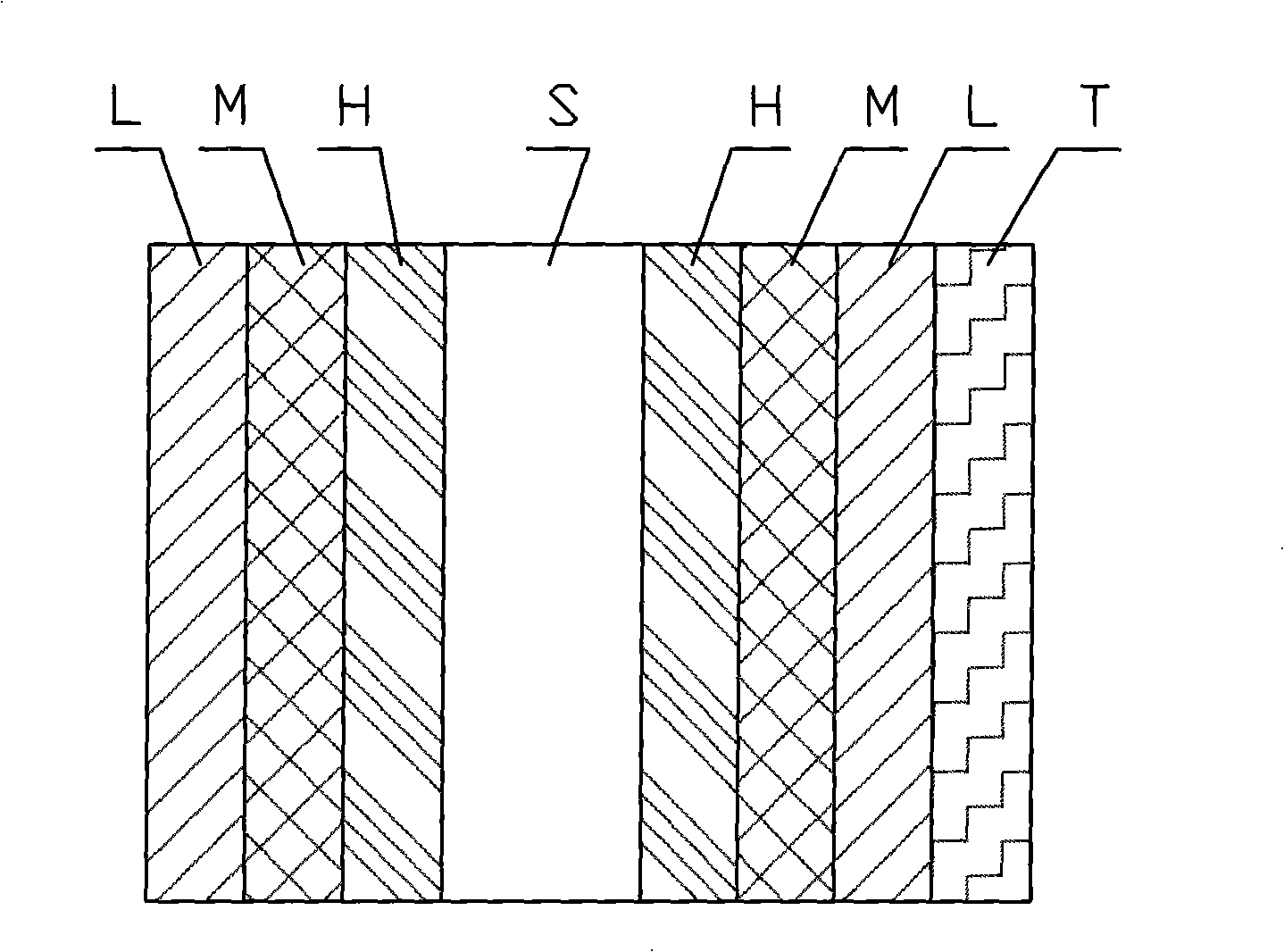
[0068] Embodiment 3: L / M / H / S / H / M / L / T type anti-reflection conductive film of the present invention
[0069] In the L / M / H / S / H / M / L / T type anti-reflection conductive film structure of the present invention, there is an extra layer of middle refractive index layer (M). This structure can realize a more stable process, and the specific film Layer features are:
[0070] The high refractive index layer (H) uses TiO 2 , the refractive index index of the material at 530nm-570nm is 2.1-2.4;
[0071] Middle refractive index layer (M), when the material is 530nm-570nm, the refractive index is 1.6-1.7;
[0072] The low refractive index layer (L) is made of SiO 2 , the refractive index of the material at 530-570nm is 1.4-1.5;
[0073] The substrate material (S) is selected from glass, and the refractive index in the visible range is 1.51-1.56;
[0074] The transparent conductive film (T) is made of ITO, and the refractive index in the visible light range is between 1.85-1.95;
[0075]...
PUM
| Property | Measurement | Unit |
|---|---|---|
| Thickness | aaaaa | aaaaa |
| Thickness | aaaaa | aaaaa |
| Thickness | aaaaa | aaaaa |
Abstract
Description
Claims
Application Information