
LED and manufacturing method thereof

A technology of light-emitting diodes and electrodes, which is applied in the direction of electrical components, circuits, semiconductor devices, etc., and can solve problems affecting the operating performance and product reliability of light-emitting diodes, poor electrical quality, and poor adhesion between the mirror surface and the epitaxial layer, etc. question

Active Publication Date: 2008-10-01
EPISTAR CORP
View PDF0 Cites 11 Cited by
  • Summary
  • Abstract
  • Description
  • Claims
  • Application Information

AI Technical Summary

Problems solved by technology

However, the light-emitting diodes manufactured by the third method usually face the problems of poor electrical quality and poor adhesion between the reflective mirror surface and the epitaxial layer, which seriously affects the operation performance and product reliability of the light-emitting diodes, and even worse lead to shortened lifetime of light-emitting diodes

Method used


Image

  • LED and manufacturing method thereof
  • LED and manufacturing method thereof
  • LED and manufacturing method thereof

Examples


Embodiment Construction

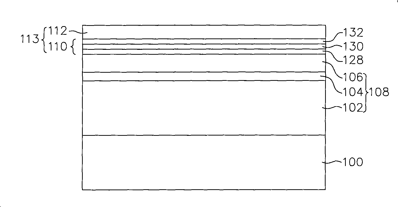
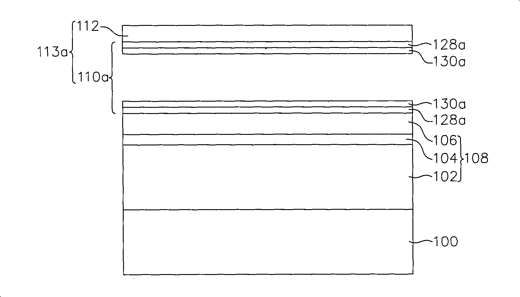
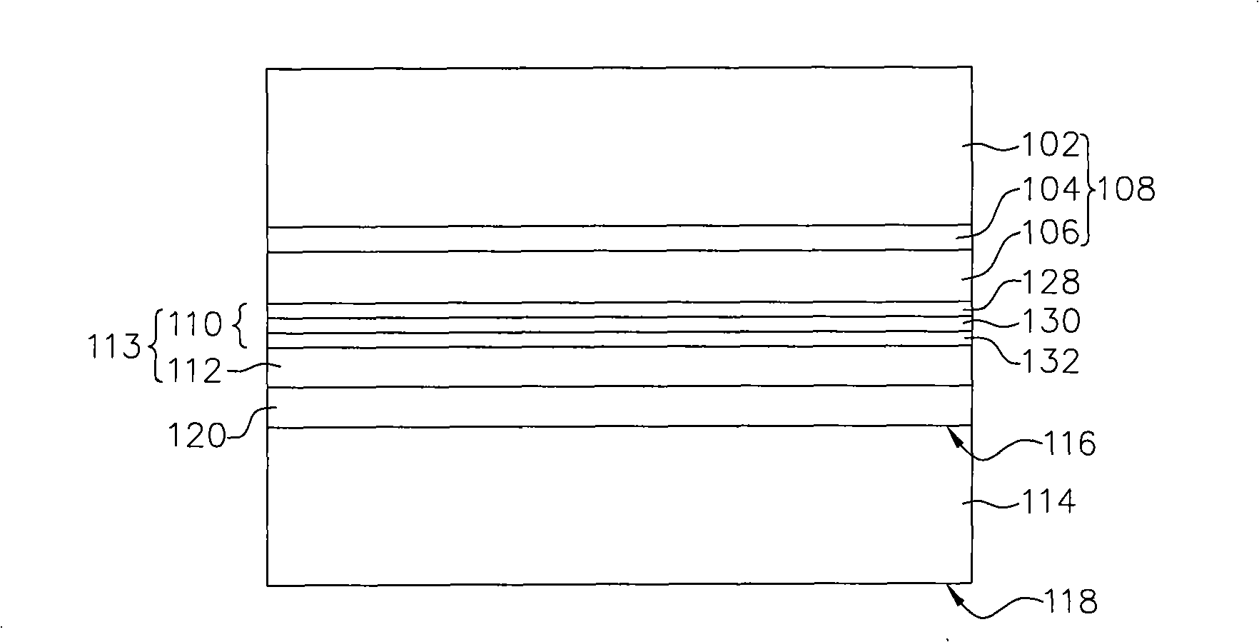
[0017] The invention discloses a light emitting diode and a manufacturing method thereof. In order to make the narration of the present invention more detailed and complete, refer to the following description and cooperate Figure 1A to Figure 6 attached drawings.

[0018] Please refer to Figure 1A to Figure 3 , which shows a cross-sectional view of a light emitting diode according to a preferred embodiment of the present invention. In an exemplary embodiment, firstly, a growth substrate 100 is provided for epitaxial growth of subsequent epitaxial materials, wherein the material of the growth substrate 100 can be, for example, sapphire, silicon carbide, silicon, zinc oxide, magnesium oxide, nitride aluminum or gallium nitride etc. Then use, for example, Metal Organic Chemical Vapor Deposition (Metal Organic Chemical Vapor Deposition; MOCVD), Liquid Phase Deposition (Liquid Phase Deposition; LPD) or Molecular Beam Epitaxy (Molecular Beam Epitaxy; MBE) to grow on the surface ...


PUM


Abstract

The invention discloses a LED and a manufacturing method thereof. The LED at least comprises: a conductive substrate with oppositely a first and a second surfaces; a reflection structure at least comprising a conductive reflection layer jointed on the conductive substrate, and a conductive dispersed Bragg reflection structure overlapped on the conductive reflection layer; a light emitting epitaxial structure arranged on the reflection structure; a first electrode arranged on part of the light emitting epitaxial structure; and a second electrode jointed with the second surface of the conductive substrate.

Description

technical field [0001] The present invention relates to a photoelectric element and its manufacturing method, and in particular to a light emitting diode and its manufacturing method. Background technique [0002] Semiconductor light-emitting elements, such as light-emitting diodes, are elements made of semiconductor materials, which are tiny solid-state light sources that can convert electrical energy into light energy. Because this kind of semiconductor light-emitting element is not only small in size, but also has the characteristics of low driving voltage, fast response rate, shock resistance, and long life, and can meet the needs of various application equipment for lightness, thinness, shortness, and smallness. Optoelectronic components that are quite common in life. [0003] At present, a fairly common method for increasing the light output of a light-emitting diode is by increasing the light extraction rate of the light-emitting diode. There are roughly the followi...

Claims


Application Information

Patent Timeline
IPC IPC(8): H01L33/00H01L33/10H01L33/36
Inventor 杨于铮郭政达黄森彬周理评
Owner EPISTAR CORP
Learn More