

Plasma processing device, plasma processing method and storage medium
A plasma and processing device technology, applied in the field of plasma processing devices, can solve labor and time-consuming problems and achieve good plasma processing effects
- Summary
- Abstract
- Description
- Claims
- Application Information
AI Technical Summary
Problems solved by technology
Method used
Image

Examples
Embodiment Construction
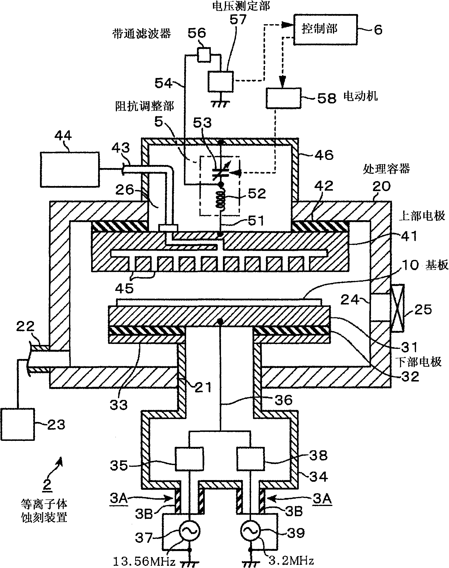
[0059] Refer below figure 1 , an embodiment in which the plasma processing apparatus of the present invention is applied to an apparatus for etching a glass substrate 10 for a liquid crystal display will be described. The plasma etching apparatus 2 has, for example, an angular tube-shaped processing container 20 made of aluminum whose surface has been anodized. A lower electrode 31 is provided at the lower center of the processing chamber 20 , and the lower electrode 31 also serves as a mounting table for placing the substrate 10 conveyed into the processing chamber 20 by a conveyance mechanism not shown. An insulator 32 is provided on the lower portion of the lower electrode 31 along the opening edge of a matching box (described later). The lower electrode 31 is sufficiently electrically floating from the processing container 20 by the insulator 32 . A matching box 34 extending downward through the opening 21 formed in the bottom wall of the processing container 20 is prov...
PUM
 Abstract
Description
Claims
Application Information