Process for decreasing deposit at reaction chamber in metal etching process

A reaction chamber and deposition technology, applied in electrical components, semiconductor/solid-state device manufacturing, circuits, etc., can solve problems such as yield impact and poor adhesion

Active Publication Date: 2008-10-15
SHANGHAI HUAHONG GRACE SEMICON MFG CORP
View PDF0 Cites 15 Cited by
  • Summary
  • Abstract
  • Description
  • Claims
  • Application Information

AI Technical Summary

Problems solved by technology

[0004] When the aluminum metal conductive layer is etched in the plasma composed of chlorine gas and boron trichloride, the patterned photoresist coating will be corroded, and the dielectric layer titanium nitride and aluminum metal will be etched. In addition to being deposited on the side walls of the aluminum metal conductive layer and th

Method used


Image

  • Process for decreasing deposit at reaction chamber in metal etching process
  • Process for decreasing deposit at reaction chamber in metal etching process
  • Process for decreasing deposit at reaction chamber in metal etching process

Examples


Embodiment Construction

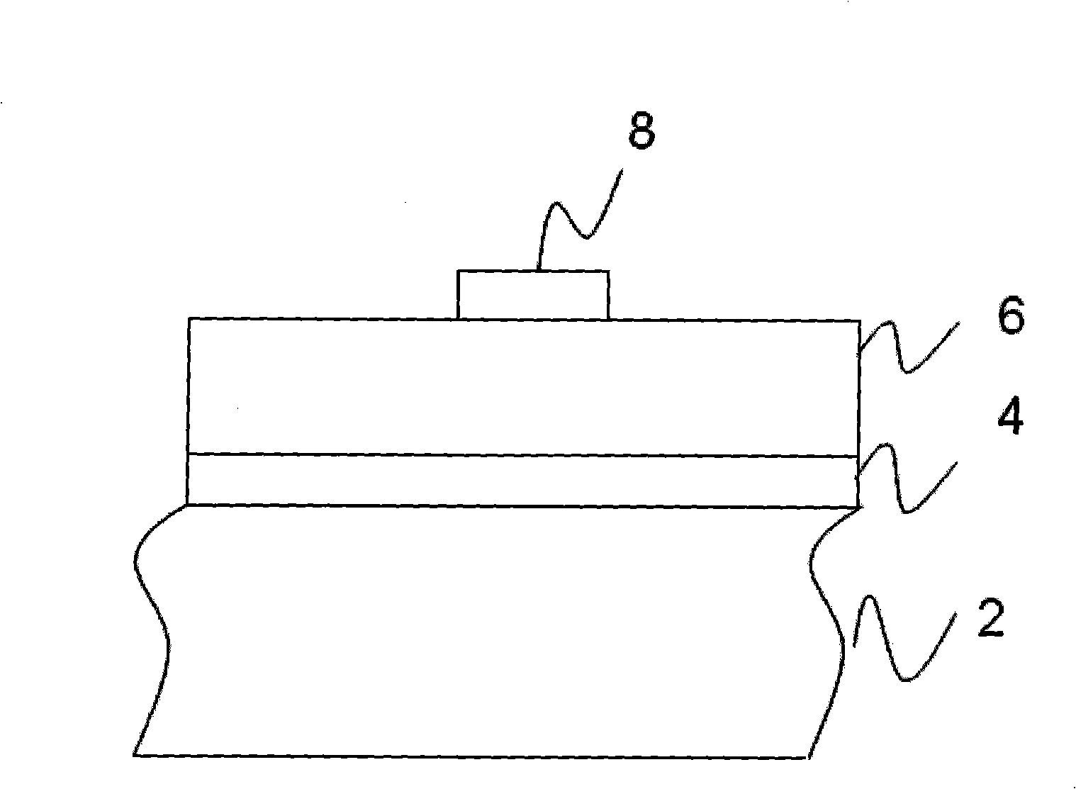
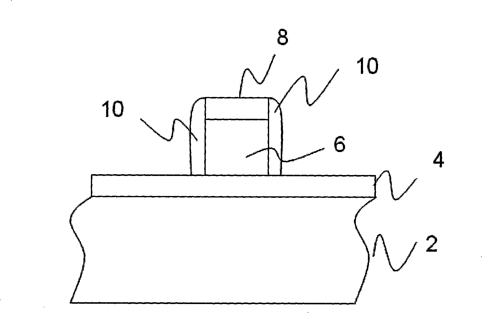
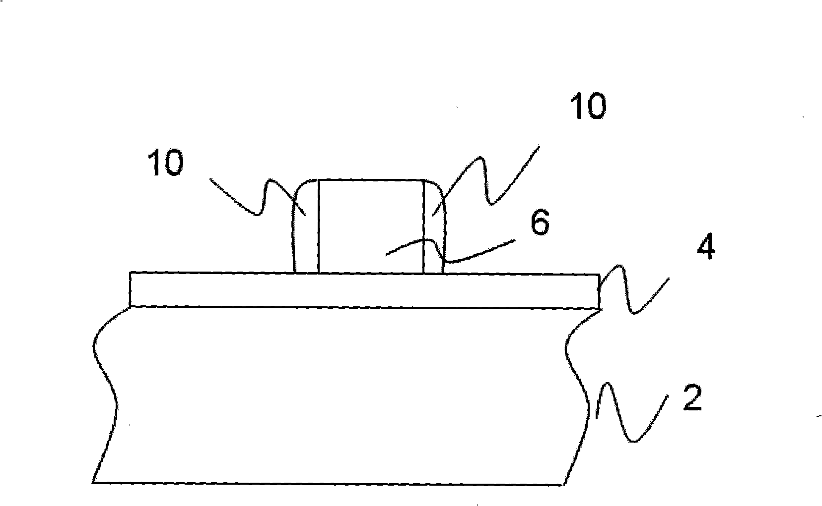
[0026] In order to explain more clearly how to reduce the deposition in the reaction chamber in the aluminum metal process, please refer to Figure 1 and figure 2 . Figure 1(a) to Figure 1(d) It is a structural cross-sectional view of carrying out the aluminum process of the present invention; figure 2 It is a schematic flow sheet of the present invention to reduce aluminum process deposit method; simultaneously refer to Fig. 1 and figure 2 Shown, the method provided by the present invention comprises the following steps:

[0027] First, step S10 is performed to provide a substrate 2 with MOS semiconductor components as shown in FIG. 4. It is usually composed of titanium nitride, and an aluminum metal conductive layer 6 is deposited on the surface of the dielectric layer 4 . Finally, a patterned photoresist coating 8 is formed on the surface of the aluminum metal conductive layer 6 .

[0028] Using the patterned photoresist coating 8 as a mask, an etching technique is u...


PUM


Abstract

The invention provides a method for reducing deposits in a reaction cavity of a metallic etching technique. The method comprises the following steps that: a dielectric layer is formed on the surface of a substrate which is provided with an MOS semiconductor component and an aluminum metal conducting layer is arranged on the dielectric layer; a patterned photoresist coating is arranged on the aluminum metal conducting layer and used as a mask for performing general etching technology; after etching is finished, carbon tetrafluoride and hydrogen nitride gas are added. The carbon tetrafluoride can reduce aluminum erosion caused by aluminium trichloride in the prior art; the carbon tetrafluoride and the hydrogen nitride gas react with polymers which are deposited on the inner wall of the reaction cavity, equipment in the reaction cavity and the sidewall of the aluminum metal conducting layer, thereby the effect of reducing the deposits can be achieved and the frequency for periodic maintenance is reduced; moreover, the mean interval for secondary cleaning is prolonged and the cost is saved.

Description

technical field [0001] The invention relates to a method for reducing deposits, in particular to a method for reducing deposits generated in a reaction chamber in an aluminum etching process. Background technique [0002] In integrated circuit manufacturing technology, metallization means that after the main body of the component is completed, according to the circuit design, it is connected through a metal film to make appropriate connections between different parts in the component or between components. Aluminum is the most widely used metal in integrated circuits. It has been used for nearly three decades. Because of its many advantages, so far, most integrated circuits still use it as a metal connection material. . The advantage of aluminum is that the resistivity of aluminum is lower than that of most metals, and a dense oxide layer (Al 2 o 3 ), will not lead to disconnection due to corrosion, which will affect the characteristics of components, coupled with the goo...

Claims


Application Information

Patent Timeline
IPC IPC(8): C23F4/00H01L21/3065H01L21/467
Inventor 张双熏
Owner SHANGHAI HUAHONG GRACE SEMICON MFG CORP
Why Eureka
Try Eureka