Lcd device and its manufacture method

A technology of a liquid crystal display device and a manufacturing method, which is applied in nonlinear optics, instruments, optics, etc., can solve the problems of weak anchoring force of liquid crystal molecules, inferior anchoring force compared to contact alignment methods, difficulties in implementation, etc., and achieve good liquid crystal response Speed, good liquid crystal alignment effect, and the effect of optimizing the yield of the manufacturing process

Inactive Publication Date: 2008-10-15
INNOLUX CORP
View PDF4 Cites 14 Cited by
  • Summary
  • Abstract
  • Description
  • Claims
  • Application Information

AI Technical Summary

Problems solved by technology

However, the alignment layer formed by photo-alignment method has weak anchoring energy for liquid crystal molecules, and cannot achieve a good alignment effect, and due to the insufficient stability of the photo-alignment material itself, the alignment ability will deteriorate over time. decrease
In addition, since this method requires high-purity (high extinction ratio) linearly polarized light, it is not easy to apply to large-sized panels, and it also has disadvantages such as

Method used


Image

  • Lcd device and its manufacture method
  • Lcd device and its manufacture method
  • Lcd device and its manufacture method

Examples


Embodiment Construction

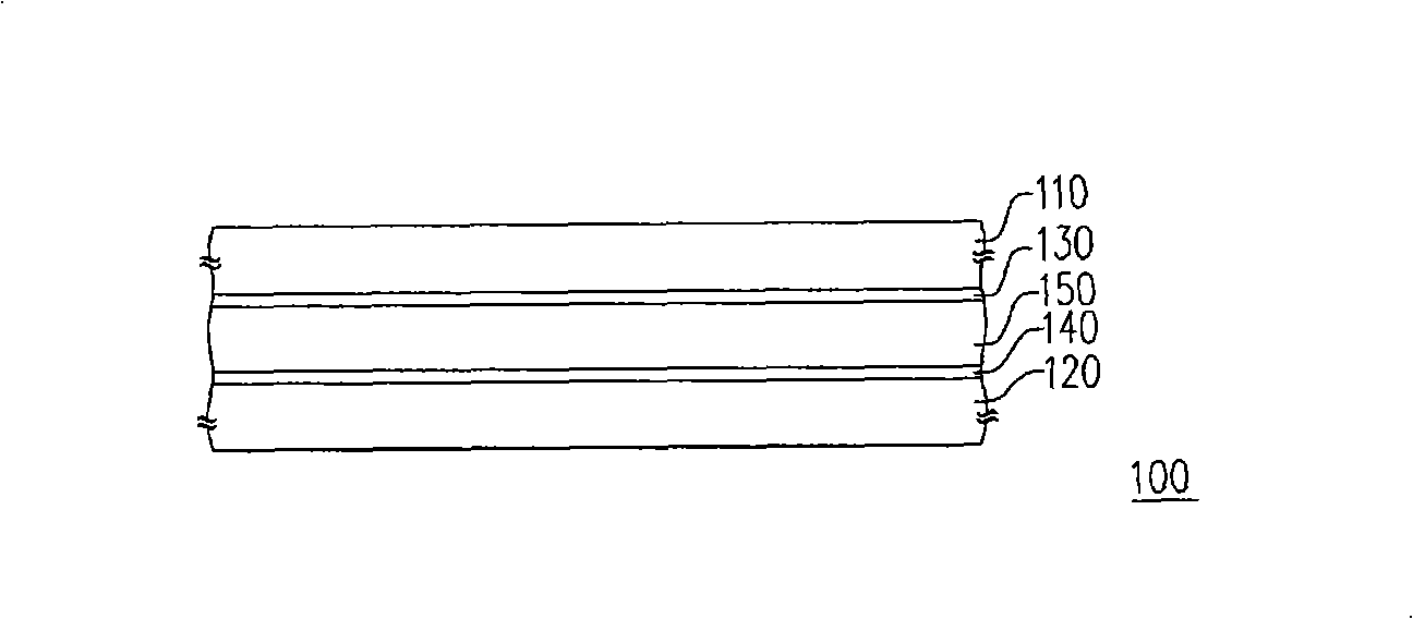
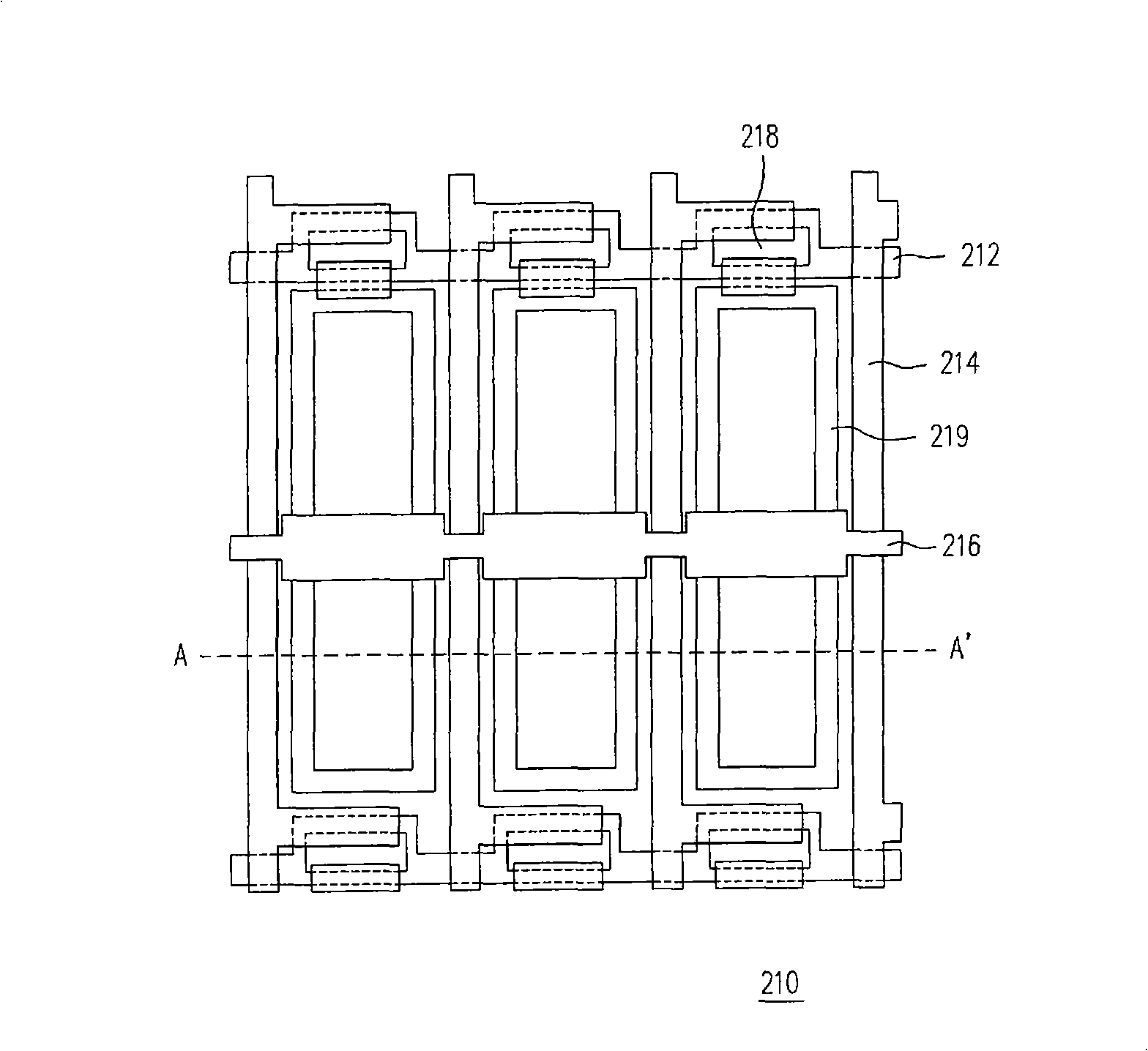
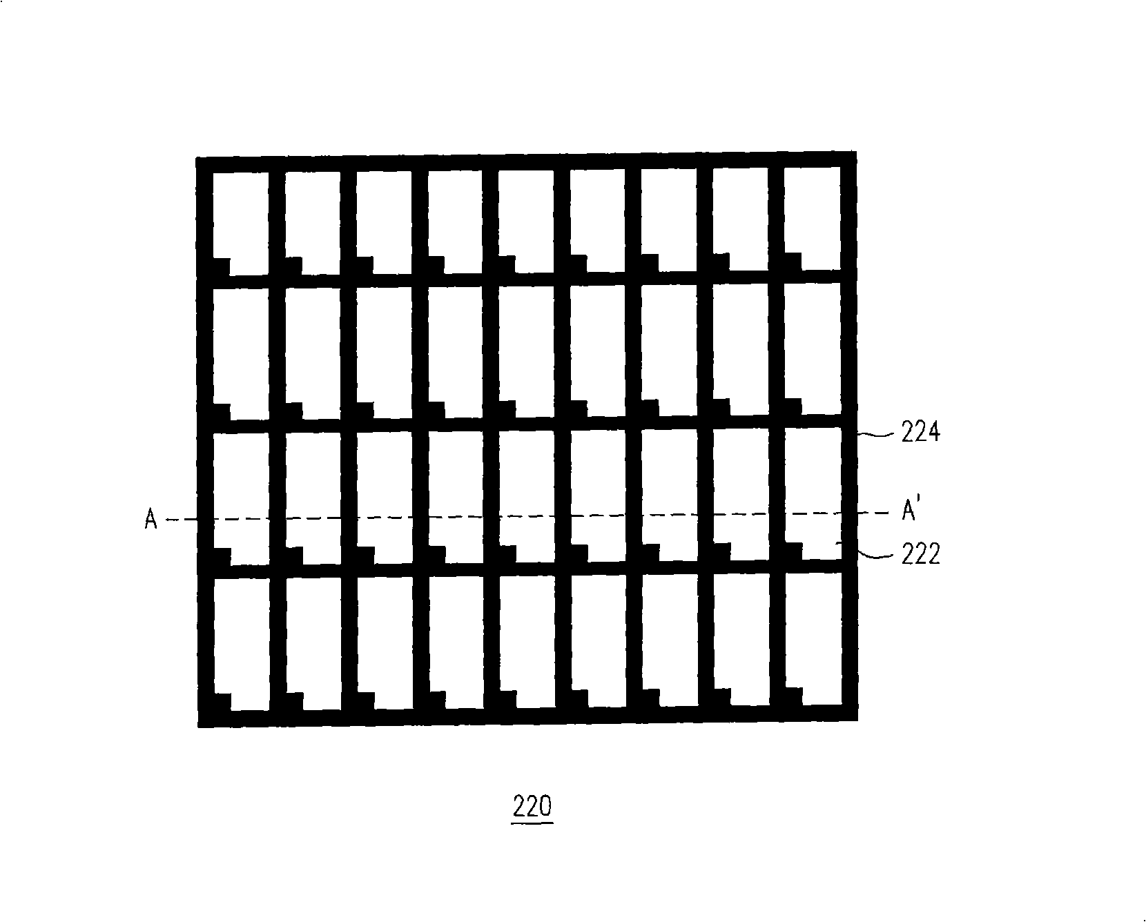
[0065] The liquid crystal display device proposed by the present invention mainly includes components such as a substrate, an opposing substrate, a liquid crystal layer, a non-contact alignment layer, and a liquid crystal stabilizing layer, wherein the substrate is, for example, a thin film transistor array substrate, and the opposing substrate is, for example, a color filter substrate The liquid crystal layer contains at least one liquid crystal molecule and is arranged between the thin film transistor array substrate and the color filter substrate. The liquid crystal display device of the present invention can be a twisted nematic liquid crystal display device (Twist Nematic LCD, TN-LCD), or a vertical alignment liquid crystal display device (Vertical Alignment LCD, VA-LCD) or other types of liquid crystal display devices , and with the different types of liquid crystal display devices, the types of liquid crystal molecules are also different, and the pre-tilt angle (pre-tilt...


PUM


Abstract

The invention relates to a liquid crystal device and a method for manufacturing the same. The liquid crystal display device comprises a substrate, a subtend substrate, a liquid crystal layer, a non-contacting alignment layer and a liquid crystal stable layer. The liquid crystal layer is provided with at least one liquid crystal molecule; the liquid crystal layer is arranged between the substrate and the subtend substrate; the non-contacting alignment layer is arranged between the substrate and the liquid crystal layer and/or between the subtend substrate and the liquid crystal layer; and the liquid crystal stable layer is arranged between the liquid crystal layer and the non-contacting alignment layer. The liquid crystal display device simultaneously combines the non-contacting alignment layer and the liquid crystal stable layer, thereby having the characteristics of providing good and stable alignment effect for the liquid crystal molecule and contributing to simultaneously improving reaction velocity and wide view angle of the liquid crystal molecule and so on.

Description

technical field [0001] The present invention relates to a display device and its manufacturing method, and in particular to a liquid crystal display device and its manufacturing method. Background technique [0002] With the substantial improvement of computer performance and the high development of Internet and multimedia technology, the volume of video or imaging devices tends to be thinner and thinner day by day. In the development of displays, with the advancement of optoelectronic technology and semiconductor manufacturing technology, liquid crystal displays (liquid crystal displays, LCDs) with superior characteristics such as high image quality, good space utilization efficiency, low power consumption, and no radiation have gradually become the market mainstream. [0003] figure 1 It is a sectional view of a liquid crystal display panel in the prior art. Please refer to figure 1 The liquid crystal display panel 100 in the prior art is mainly composed of an opposite...

Claims


Application Information

Patent Timeline
IPC IPC(8): G02F1/1337G02F1/1333
Inventor 吴阜苍高振宽李恒贤庄正旭
Owner INNOLUX CORP
Why Eureka
Try Eureka