Flash memory and preparation method thereof

A manufacturing method and memory technology, applied in semiconductor/solid-state device manufacturing, electric solid-state devices, semiconductor devices, etc., can solve problems such as insufficient isolation, and achieve the effect of preventing short-circuit channels

Active Publication Date: 2008-10-22
SEMICON MFG INT (SHANGHAI) CORP +1
View PDF1 Cites 9 Cited by
  • Summary
  • Abstract
  • Description
  • Claims
  • Application Information

AI Technical Summary

Problems solved by technology

[0007] The problem solved by the present invention is that in the existing SONOS flash memory technology, due to insufficient isolation between the bit line, the word line and the semiconductor substrate, multiple short-circuit channels are formed

Method used


Image

  • Flash memory and preparation method thereof
  • Flash memory and preparation method thereof
  • Flash memory and preparation method thereof

Examples


Embodiment Construction

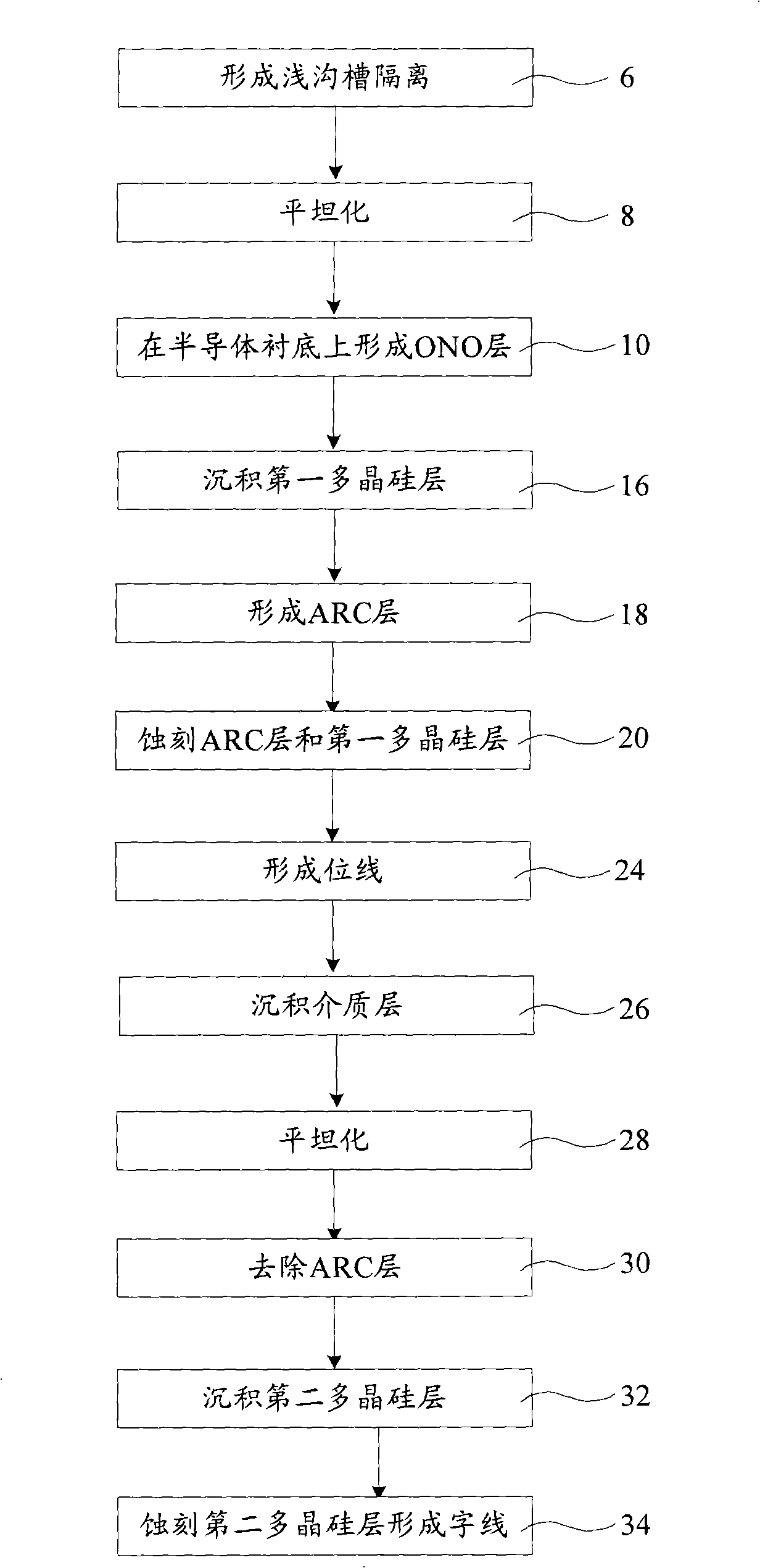
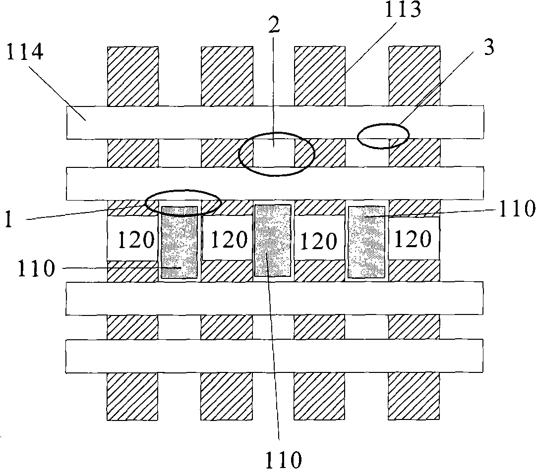
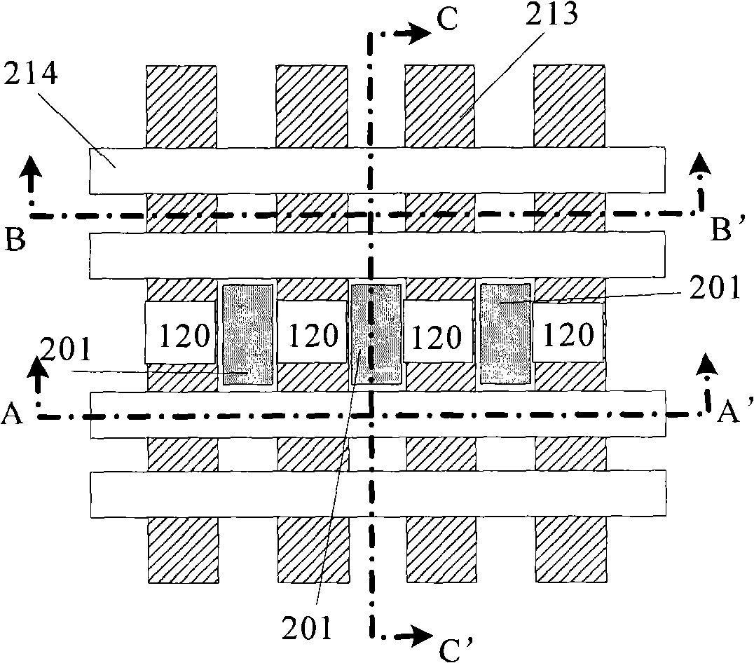
[0026] The present invention provides a flash memory and a manufacturing method thereof. In this embodiment, in the manufacturing process of the SONOS flash memory, the three-layer stack structure of the medium layer-trapping charge layer-dielectric layer of the SONOS flash memory is reserved in the area other than the word line And form sidewalls on both sides of the word line, fully between the word line and the word line, between the bit line and the bit line, between the word line and the bit line, around the shallow trench isolation and between the word line and the semiconductor substrate Isolation is carried out to prevent the formation of short-circuit channels and cause leakage current.

[0027]The present invention firstly provides a method for manufacturing a SONOS flash memory, comprising: providing a semiconductor substrate, on which there is a three-layer stacked structure consisting of a dielectric layer-charge-trapping layer-dielectric layer, a first polysilicon...


PUM


Abstract

The invention relates to a method for manufacturing a flash memory. The method comprises the following steps that: a second polysilicon layer and a second etching barrier layer are etched in turn along the direction of word lines until dielectric layers are exposed; the word lines are formed and a three-layered stacking structure on the area outside the word lines is reserved; sidewalls are formed on both sides of the word lines; the second etching barrier layer is removed, transition metals are formed on the second polysilicon layer and the dielectric layer and react with the word lines through annealing to form a silicide layer; and residual transition metals which do not react are removed and the SONOS flash memory is formed. The method fully insulates word lines and word lines, word lines and bit lines, and word lines and a semiconductor substrate through preservation of the three-layered (a dielectric layer-a capture charge layer-a dielectric layer) stacking structure of the SONOS flash memory and formation of the sidewalls on both sides of the word lines when the SONOS flash memory is manufactured, and prevents formation of a short-circuit channel and generation of drain current.

Description

technical field [0001] The invention relates to a manufacturing method of a flash memory, in particular to a SONOS flash memory and a manufacturing method thereof. Background technique [0002] In general, semiconductor memories used to store data are classified into volatile memories and nonvolatile memories, volatile memories are prone to lose their data when power is interrupted, and nonvolatile memories are retained even after the power supply is turned off On-chip information. Compared with other non-volatile storage technologies (eg, disk drives), non-volatile semiconductor memories are characterized by low cost and high density. Therefore, non-volatile memory has been widely used in various fields, including embedded systems, such as PCs and peripherals, telecommunication switches, cellular phones, network interconnection equipment, instrumentation and automotive devices, as well as emerging voice, image , Data storage products such as digital cameras, digital voice...

Claims


Application Information

Patent Timeline
Patent Type & Authority Applications(China)
IPC IPC(8): H01L21/8247H01L21/768H01L27/115H01L23/522
Inventor 蔡信裕刘经国衣冠君陈自凡
Owner SEMICON MFG INT (SHANGHAI) CORP
Why Eureka
Try Eureka