Digital microcurrent-controlled device and control method based on electrowetting effect on dielectric

A digital microfluidic and electrowetting technology, applied in chemical method analysis, instruments, scientific instruments, etc., can solve the problems of high droplet driving voltage, high production cost, unfavorable integration of chips and IC circuits, etc.

Inactive Publication Date: 2008-10-29
FUDAN UNIV
View PDF0 Cites 42 Cited by
  • Summary
  • Abstract
  • Description
  • Claims
  • Application Information

AI Technical Summary

Problems solved by technology

[0017] However, in the current microfluidic devices, the voltage for driving droplets is relatively high, which is not conducive to the integration of chips and IC circuits, and the manufacturing process is more complicated and the manufacturing cost is higher.

Method used


Image

  • Digital microcurrent-controlled device and control method based on electrowetting effect on dielectric
  • Digital microcurrent-controlled device and control method based on electrowetting effect on dielectric
  • Digital microcurrent-controlled device and control method based on electrowetting effect on dielectric

Examples


Embodiment Construction

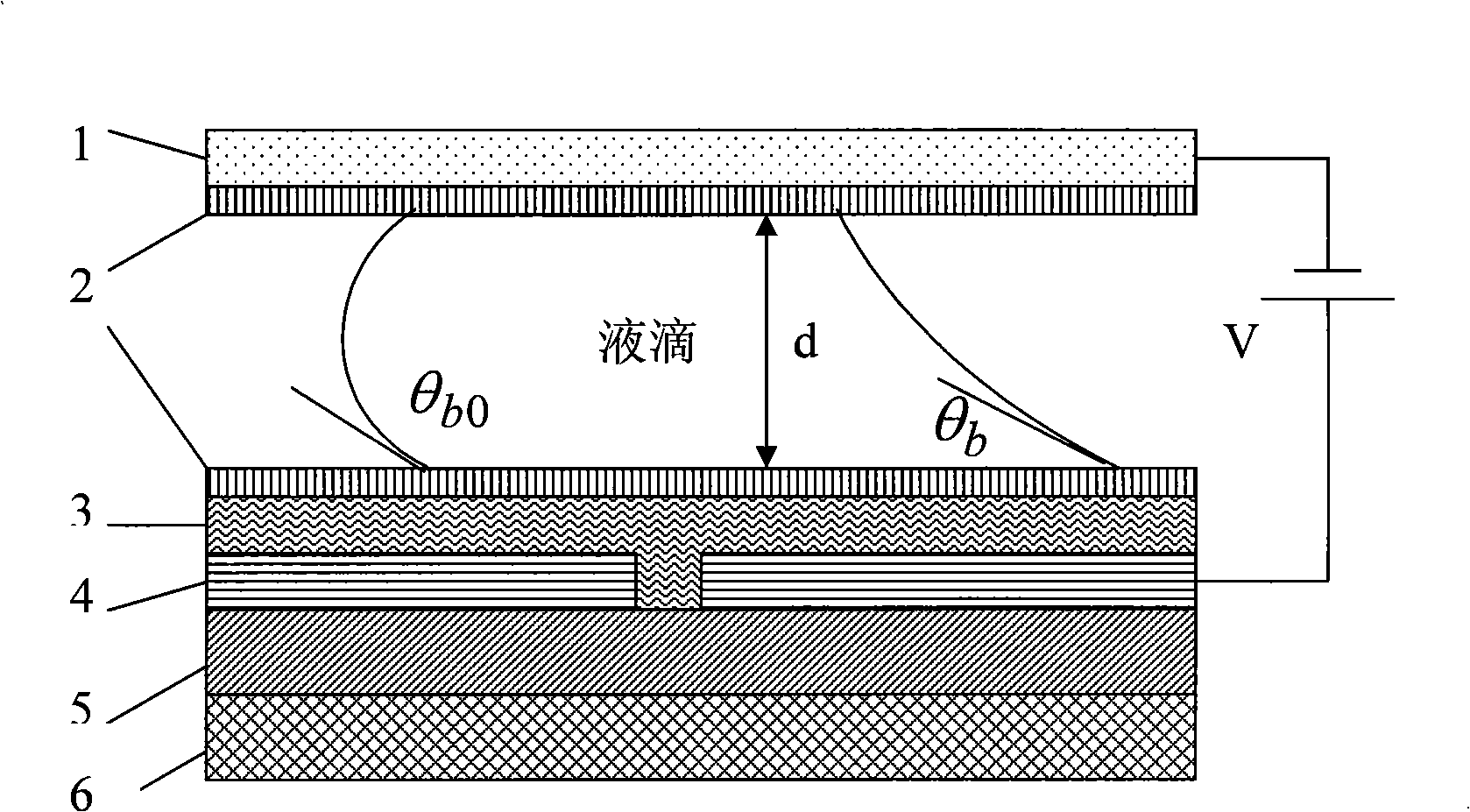
[0029] The invention only needs a simple four-step process to realize the digital microfluidic control function of the droplet, greatly reducing the steps and complexity of the process. The reduction of the operating voltage is also beneficial to the compatibility with the integrated circuit technology, and helps to realize the system integration with the micro-detection.

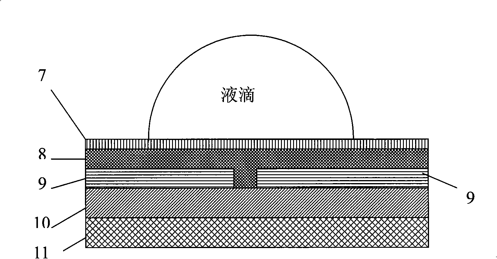
[0030] The specific technological process of the microfluidic device of the present invention is as follows: first, a silicon dioxide layer with a thickness of 700-1000nm is generated by thermal oxidation on the silicon substrate as an insulating layer; secondly, a metal Al layer is evaporated and deposited on the insulating layer, with a thickness of 150-300nm, wet etching to form an electrode pattern; then spin-coat a layer of high dielectric constant organic film (such as P(VDF-TrFE) at a speed of 800-1000 rpm, bake to remove the organic solvent, and form a stable Dielectric layer, the dielectric constan...


PUM

PropertyMeasurementUnit
widthaaaaaaaaaa
thicknessaaaaaaaaaa

Abstract

The invention belongs to the digital microfluidic technical field, in particular relates to a digital microfluidic device and control method based on the electrowetting effect of dielectric; the device structure of the invention comprises a substrate, an insulating layer, a metal electrode layer, a dielectric layer and a drainage layer in sequence from bottom to top, wherein, the dielectric layer adopts high dielectric constant material, such as an organic film of PVDF, etc.; the electrode adopts a single-layer control electrode; a liquid drop driving method based on the device is that the liquid drop is added on the surface of the drainage layer of the upper of two adjacent electrodes at the same layer, voltage is applied between the two electrodes, the controlled movement of the liquid drop can be realized by moving the two electrodes; the digital microfluidic device and control method of the invention reduce the complexity of the technique largely, reduce the cost and increase the flexibility of the microfluidic operation.

Description

technical field [0001] The invention belongs to the technical field of digital microfluidics, and in particular relates to a digital microfluidic device and a control method thereof. Background technique [0002] In the past ten years, the concept of "Lab-on-a-chip" (Lab-on-a-chip) has been rapidly developed and realized. It is a micro-analytical instrument realized by using micro-processing and integration technology combined with various analysis and detection principles. , has the advantages of small size, low power consumption, high sensitivity, and portability, and can be widely used in biological, medical, and chemical detection, and has applications in national security, immune detection, environmental protection, food hygiene, genetic screening, disease diagnosis, etc. potential. [0003] Regardless of the object of its analysis and detection, the structural composition of the "lab-on-a-chip" is divided into two basic modules: "sample processing" (such as sample inp...

Claims


Application Information

Patent Timeline
Patent Type & Authority Applications(China)
IPC IPC(8): G01N35/00G01N35/08G01N31/00
Inventor 赵平安李寅青周嘉刘冉
Owner FUDAN UNIV
Why Eureka
Try Eureka