Charge pump construction for phase lock loop circuit

A charge pump and phase-locked loop technology, applied in the field of phase-locked loop circuit charge pump structure, can solve the problems of loss of lock, phase-locked loop output signal jitter, phase-locked loop noise, etc., to achieve small errors, reduce the degree of mismatch, The effect of eliminating the influence of parasitic capacitance

Active Publication Date: 2008-11-19
ARKMICRO TECH
View PDF0 Cites 21 Cited by
  • Summary
  • Abstract
  • Description
  • Claims
  • Application Information

AI Technical Summary

Problems solved by technology

[0011] In order to solve the problems existing in the charge pump structure of the above-mentioned phase-locked loop circuit, the present invention proposes a charge pump structure applied to the phase-locked loop circuit, which is used

Method used


Image

  • Charge pump construction for phase lock loop circuit
  • Charge pump construction for phase lock loop circuit
  • Charge pump construction for phase lock loop circuit

Examples


Example Embodiment

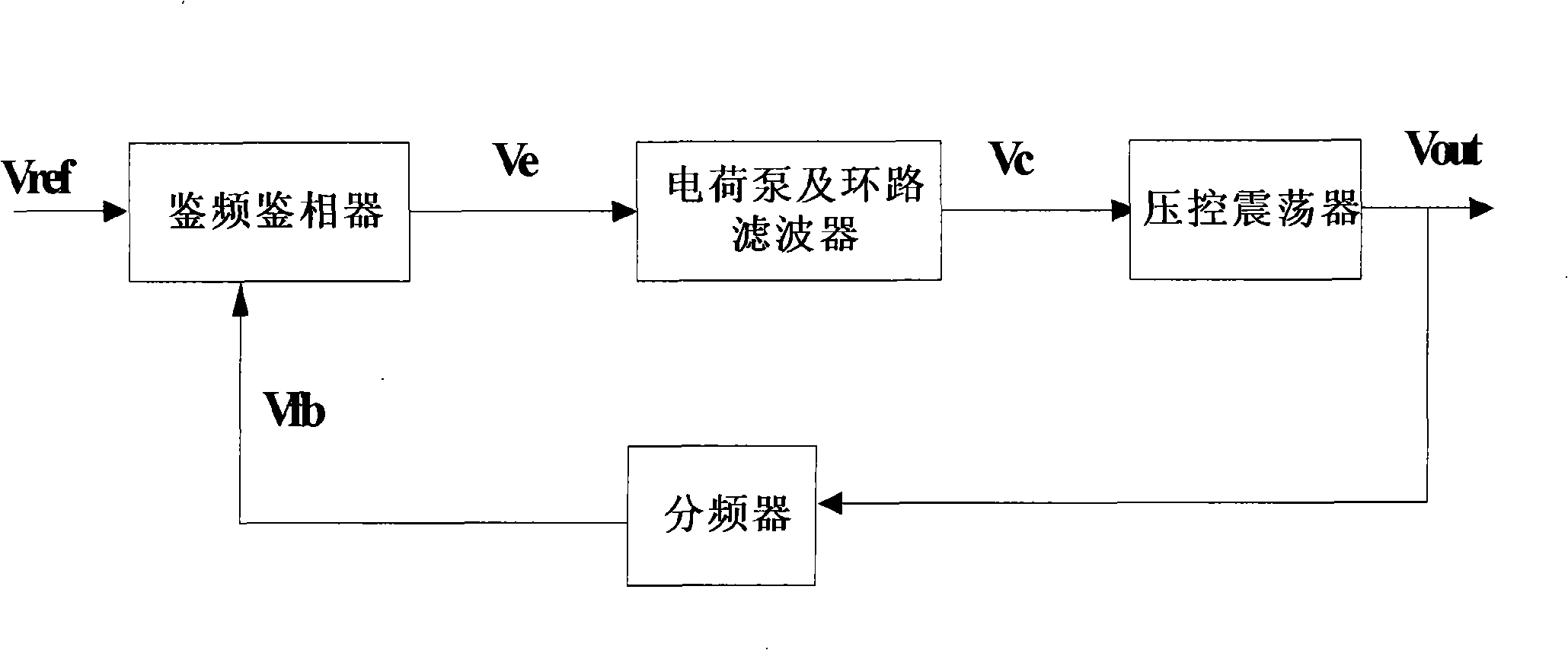
[0027] Such as Figure 4 As shown, the present invention discloses a charge pump structure for a phase-locked loop circuit, which includes two identical single-ended variable differential signal buffer units to generate two complementary differential signals from the Up and Down signals, and Their gate delay and connection delay are the same, and a symmetrical and balanced charge pump. The switch tube of the charge pump is controlled by the differential signal of the buffer unit. The Up and Down signals generated by the phase discriminator unit of the frequency discriminator are first passed through the differential signal. The generating unit generates two pairs of differential signals S1, S3 and S2, S4, and then controls the switch tube of the charge pump unit.

[0028] Figure 5 It is a specific circuit block diagram of the differential signal generating unit of the phase-locked loop circuit of the present invention, which includes a circuit composed of two sets of the same gat...


PUM


Abstract

The invention discloses a charge pump structure for a phase-locked loop circuit, which is used to convert the phase difference signal output by a frequency discriminator or phase detector to the voltage signal so that to control the output signal frequency of a VCO(voltage controlled oscillator). The invention is characterized in that the charge bump structure includes two identical buffer units which is used to convert the single end signal to differential signal and can generate two complementary differential signals on the Up signal and Down signal, and a charge and loop filter unit which are formed by two identical charge pump circuits connected in series and are used to convert the complementary differential signal to the voltage signal. The charge pump structure of the invention eliminates the influence of parasitic capacitance, reduces the mismatch degree of the transistor during manufacture and keeps the relative matching of the transistor.

Description

technical field [0001] The invention relates to a phase-locked loop circuit structure applied to image display system pixel clock recovery, in particular to a phase-locked loop circuit charge pump structure with noise suppression capability. Background technique [0002] Phase locked loop circuit (phase locked loop, PLL) is an automatic control circuit system that can track the frequency and phase of the input signal, and track and lock the phase and frequency of the output signal and the input signal, so that the phase and frequency of the output signal Can be fixed at a preset value or range. It is widely used in computers, communications, and consumer electronics products. Its main functions are frequency synthesis, clock or data recovery, and signal error elimination. [0003] Initially, DeBellescize proposed the synchronous detection theory in 1932, and published the description of the phase-locked loop circuit for the first time, but it did not attract widespread atte...

Claims


Application Information

Patent Timeline
IPC IPC(8): H03L7/08
Inventor 胡江鸣刘敬波王韧秦玲李敏吴才润常军锋石岭
Owner ARKMICRO TECH
Why Eureka
Try Eureka