Predetermined pattern manufacturing method

A technology of predetermined pattern and production method, applied in conductive pattern formation, printed circuit manufacturing, electrical components, etc., can solve problems such as insufficient uniformity, inaccurate predetermined pattern, environmental pollution, etc.

Inactive Publication Date: 2008-11-19
CHUANG YEOU IND
View PDF0 Cites 20 Cited by
  • Summary
  • Abstract
  • Description
  • Claims
  • Application Information

AI Technical Summary

Problems solved by technology

[0005] The main purpose of the present invention is to provide a method for making a predetermined pattern, which uses a laser to etch a predetermined line, so as to solve the environme

Method used


Image

  • Predetermined pattern manufacturing method
  • Predetermined pattern manufacturing method
  • Predetermined pattern manufacturing method

Examples


Embodiment Construction

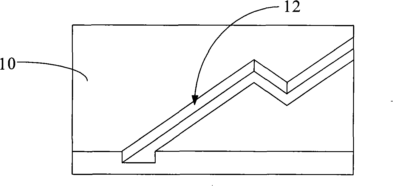
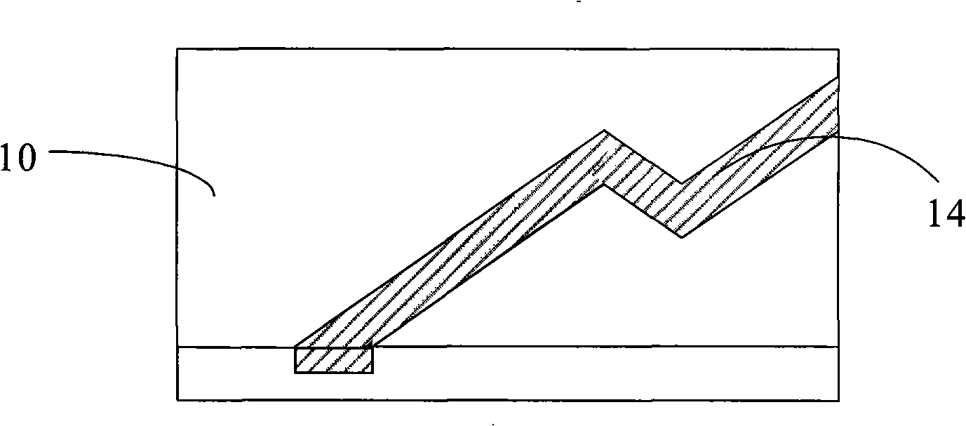
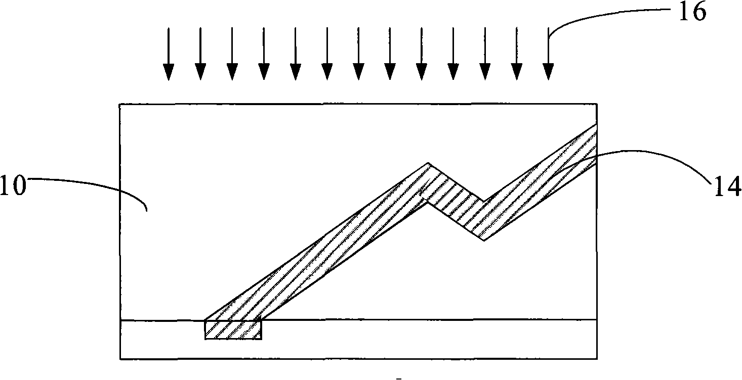
[0019] Please refer to FIGS. 1A-1C . FIGS. 1A-1C are schematic diagrams of a method for making a predetermined pattern according to the present invention. As shown in FIG. 1C , the manufacturing method of the predetermined pattern of the present invention mainly can form the predetermined pattern on the insulating substrate 10 of the printed circuit board. In addition to the circuit 14 shown in FIG. 1C , the predetermined pattern can also be a mark (such as a serial number of a product, a name of a manufacturer, etc.), and an alignment hole.

[0020] To put it simply, in the method for making the predetermined pattern of the present invention, it is first necessary to provide the insulating substrate 10 of the printed circuit board, and according to the design of the predetermined pattern, the predetermined pattern ( Such as line, product serial number, manufacturer's name, etc.). The following will take the fabrication of the circuit 14 as shown in FIG. 1C as an example for ...


PUM


Abstract

The invention discloses a fabrication method for a predetermined pattern, which is mainly used for fabricating the predetermined pattern on a printed circuit board. The method of the invention comprises that according to the design of the predetermined pattern, the predetermined pattern is etched in the insulating base plate of the provided printed circuit board by utilizing the non-chemical etched laser beam. If the predetermined pattern is a line, the metallization treatment further performed to the etched predetermined pattern, and the required line can be formed. By using the accurately controlled laser etching, not only the chemical pollution does not caused, simultaneously, the required pattern can be accurately etched, but also the uneven and inaccurate thickness phenomenon does not occur.

Description

technical field [0001] The invention relates to a method for making a predetermined pattern, especially the predetermined pattern made on a printed circuit board. Background technique [0002] The printed circuit board is a circuit board composed of drawing the electrical wiring connecting the circuit parts into a wiring pattern according to the circuit design, and then reproducing the electrical conductor on the insulator by the mechanical processing and surface treatment specified by the design. In the prior art, the copper foil layer is first pasted on the insulating substrate on the printed circuit board, and then a predetermined pattern (such as circuit, alignment hole, mark, etc.) is formed by using procedures such as development and etching. [0003] However, with the increasingly stringent requirements for environmental protection, the technology used to form the predetermined pattern in the existing technology will bring high pollution chemical etching, and it must ...

Claims


Application Information

Patent Timeline
IPC IPC(8): H05K3/00H05K3/10
Inventor 张宗贵
Owner CHUANG YEOU IND
Why Eureka
Try Eureka