Multi-layer high quality gate dielectric for low-temperature poly-silicon tfts

A gate dielectric layer, dielectric layer technology, applied in the direction of coating, solid diffusion coating, metal material coating process, etc., can solve the problems of inapplicability, soft glass size, instability, etc.

Inactive Publication Date: 2008-11-19
APPLIED MATERIALS INC
View PDF15 Cites 8 Cited by
  • Summary
  • Abstract
  • Description
  • Claims
  • Application Information

AI Technical Summary

Problems solved by technology

Since the high-temperature deposition process will cause the dopant to diffuse inside the deposited film layer, the high-temperature deposition process (for example, higher than 600°C) cannot be used to form a good interface between the deposited film layer and the p-Si channel layer. And it may not be suitable for glass substrates with thin films deposited on it because the glass may become soft and cause dimensional instability

Method used


Image

  • Multi-layer high quality gate dielectric for low-temperature poly-silicon tfts
  • Multi-layer high quality gate dielectric for low-temperature poly-silicon tfts
  • Multi-layer high quality gate dielectric for low-temperature poly-silicon tfts

Examples


Embodiment Construction

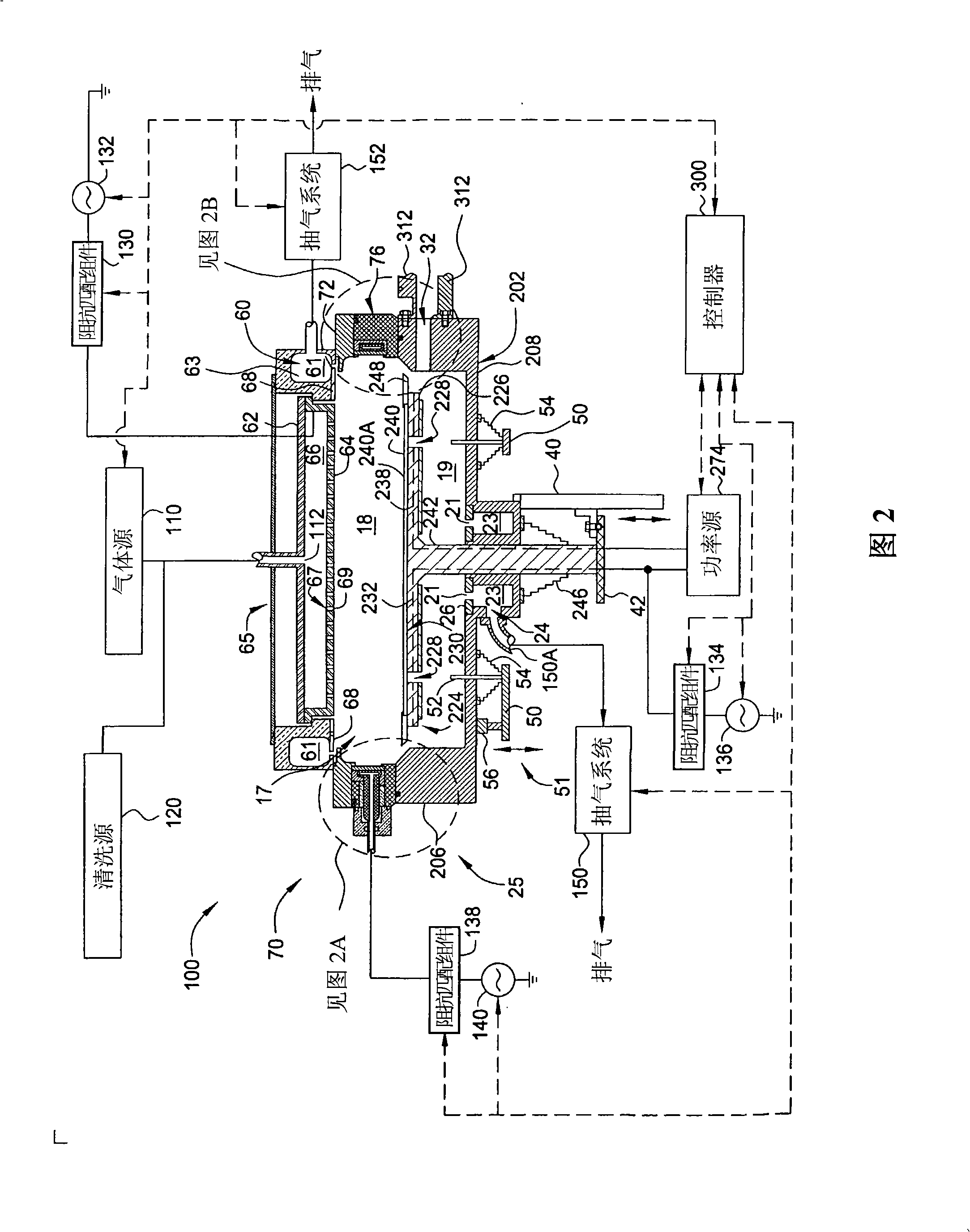
[0061] The invention provides a device and a method for treating the surface of a substrate by using inductively coupled high-density plasma. In general, the concepts of the present invention can be applied to flat panel display manufacturing processes, semiconductor manufacturing processes, solar cell manufacturing processes, or any other substrate manufacturing processes. The present invention will be described exemplarily with reference to a chemical vapor deposition system for processing large-area substrates, such as a plasma-enhanced chemical vapor deposition (PECVD) system available from AKT Corporation; AKT is located in Santa Maria, California. Monica's Applied Material company belongs to the unit. It should be understood, however, that the apparatus and method may also be applicable in other systems, including systems for processing circular substrates.

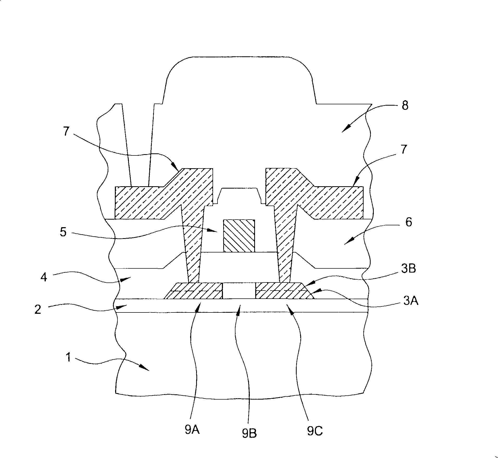
[0062] figure 1 A cross-sectional view showing a thin film transistor structure; the optically transparent subs...


PUM


Abstract

A method and apparatus that is useful for forming a high quality gate dielectric layer in MOS TFT devices using a high density plasma oxidation (HDPO) process. In one embodiment a HDPO process layer is formed over the channel, source and drain regions to form a dielectric interface and then one or more dielectric layers are deposited on the HDPO layer to form a high quality gate dielectric layer. The HDPO process generally uses an inductively and / or capacitively coupled RF transmitting device to generate and control the plasma generated over the substrate and injecting a gas containing an oxidizing source to grow the interfacial layer. A second dielectric layer may then be deposited on the substrate using a CVD or PECVD deposition process. Aspects of the invention also provide a cluster tool that contains at least one specialized plasma processing chamber that is capable of depositing a high quality gate dielectric layer.

Description

technical field [0001] Embodiments of the present invention relate to an apparatus and method for manufacturing electronic components using a plasma processing system. Background technique [0002] Metal interconnects and other features are formed by depositing and removing layers of conductive, semiconducting, and dielectric materials on glass substrates in the fabrication of flat panel displays (FPDs), thin film transistors (TFTs), and liquid crystal cells. The resulting various features are integrated in a system to produce an active matrix display screen in which the display state is generated in each pixel on the FPD. The manufacturing process technologies used to produce FPDs include plasma-enhanced chemical vapor deposition (PECVD), physical vapor deposition (PVD), etching, and the like. Plasma processing is particularly suitable for the production of flat panel displays because it requires relatively low manufacturing process temperatures during the deposition of th...

Claims


Application Information

Patent Timeline
Patent Type & Authority Applications(China)
IPC IPC(8): C23C14/16
CPCC23C16/0218C23C8/36C23C16/402C23C16/50C23C16/00
Inventor 约翰·怀特
Owner APPLIED MATERIALS INC
Why Eureka
Try Eureka