Aluminum cushion layer etching method and bump formation method

A technology of etching aluminum and pads, which is applied in the manufacture of electrical components, electrical solid devices, semiconductor/solid devices, etc., can solve problems affecting the yield of shipment inspection, increase of leakage current contact resistance, surface roughness, etc., to avoid Effect of surface roughness on aluminum underlayment

Inactive Publication Date: 2008-11-26
SEMICON MFG INT (SHANGHAI) CORP +1
View PDF1 Cites 10 Cited by
  • Summary
  • Abstract
  • Description
  • Claims
  • Application Information

AI Technical Summary

Problems solved by technology

However, after research, it was found that after the aluminum pad layer was etched using the existing technology, the surface of the rewiring layer formed on the

Method used


Image

  • Aluminum cushion layer etching method and bump formation method
  • Aluminum cushion layer etching method and bump formation method
  • Aluminum cushion layer etching method and bump formation method

Examples


Embodiment Construction

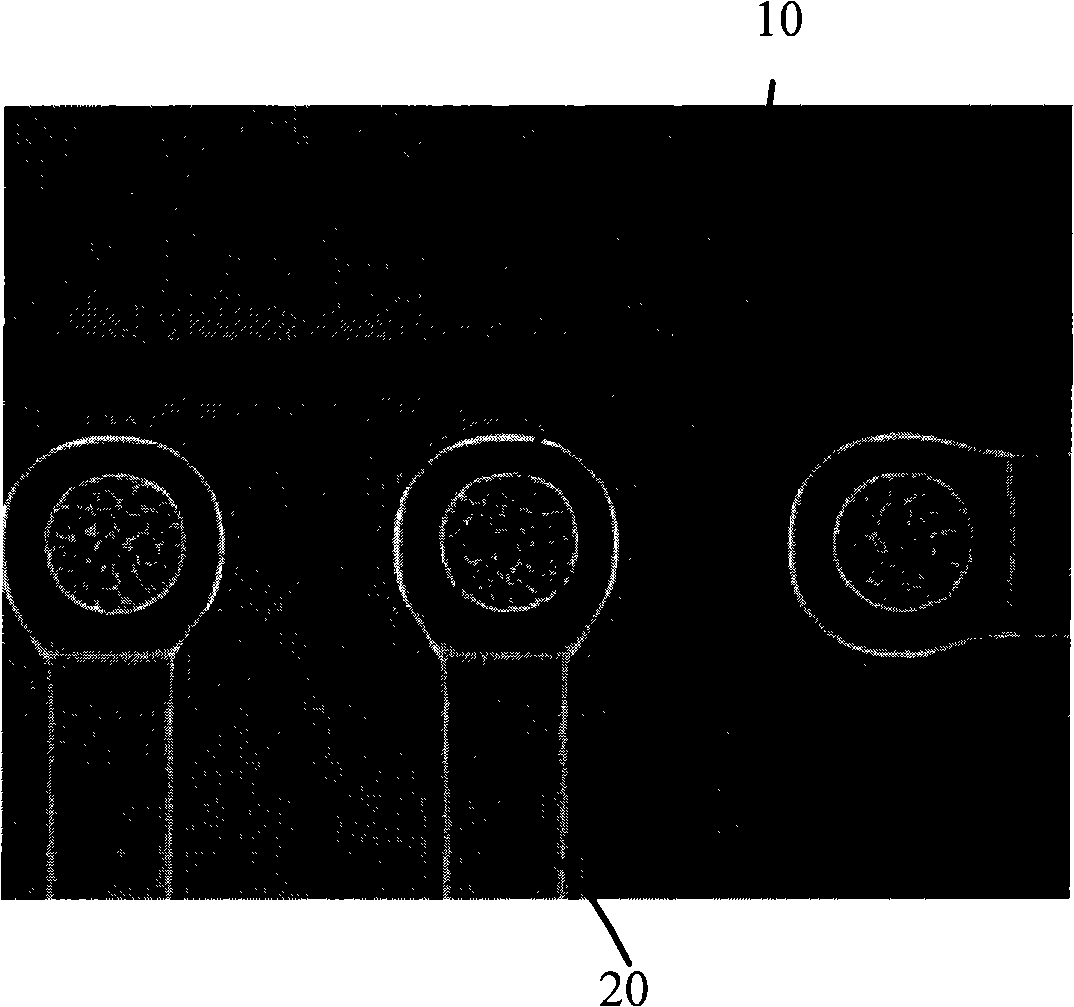
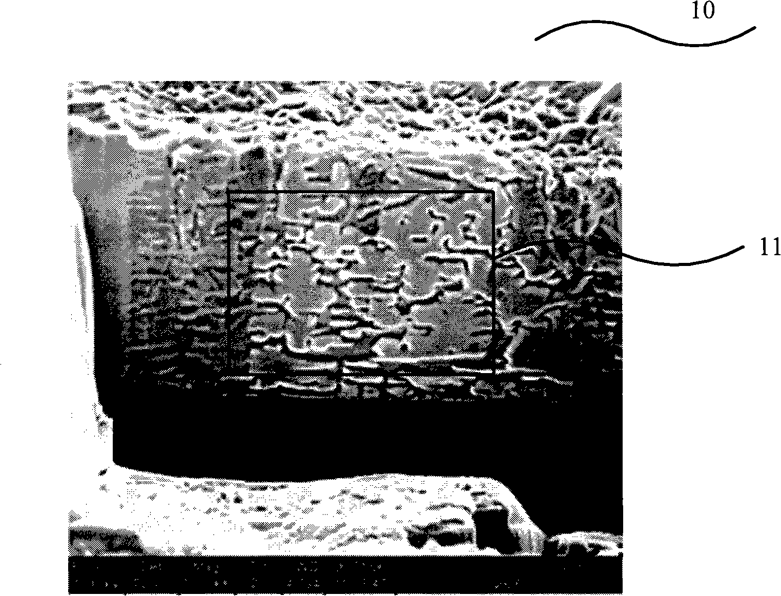
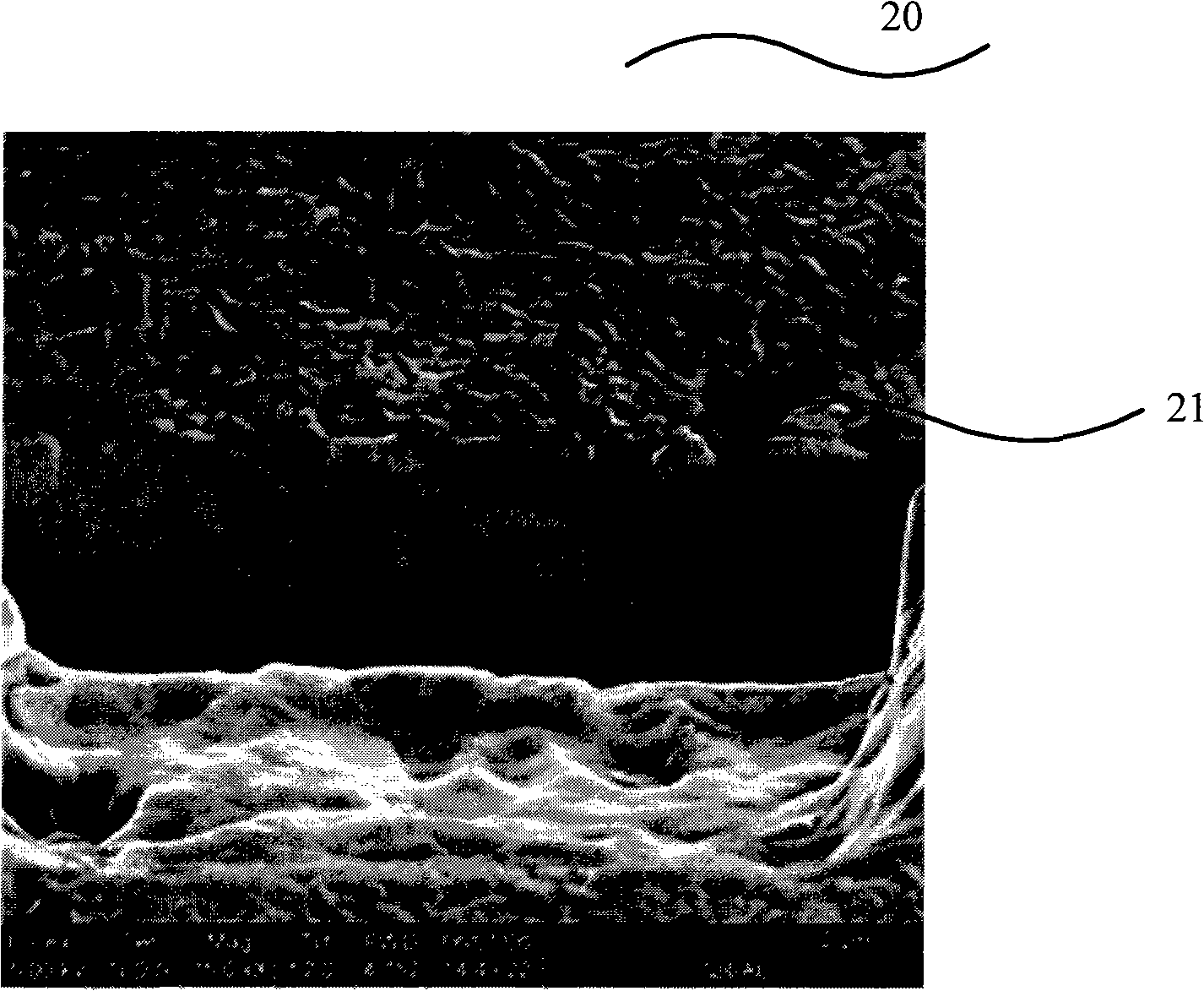
[0030] The invention provides a method for etching an aluminum underlayment, which uses a generation power (MF) ranging from 600 to 800W to generate plasma, and an acceleration power (RF) ranging from 100 to 600W to accelerate the plasma to remove the oxide layer on the surface of the aluminum underlayment and contamination, etc., the present invention also provides a method for forming bumps. Compared with the prior art, the present invention reduces the impact on the surface roughness of the aluminum pad layer by reducing the range of generating power (MF) for generating plasma and reducing the range of accelerating power (RF) for accelerating plasma, thereby achieving The roughness of the rewiring layer subsequently formed on the aluminum pad layer is reduced during the bump formation process.

[0031] The present invention first provides a method for etching an aluminum pad, comprising: providing a semiconductor substrate; forming an aluminum pad, a passivation layer and a...


PUM


Abstract

A method for etching an aluminum pad layer comprises providing a semiconductor substrate, forming an aluminum pad layer, a passivating layer and a dielectric layer on the semiconductor substrate, wherein the aluminum layer is inlaid in the passivating layer and exposes through the passivating layer and a first opening of the dielectric layer, and further utilizing argon plasma to etch the aluminum pad layer, wherein the production power (MF) for generating the argon plasma is arranged between 600W and 800W, the accelerating power (RF) for accelerating the argon plasma is arranged between 100W and 600W, and the etching time is arranged between 55s and 100s. The invention further provides a method for forming bumps. Compared with the prior art, the method for etching an aluminum pad layer reduces the generation power (MF) for generating the argon plasma, the accelerating power (RF) for accelerating the argon plasma and the time to etch the aluminum pad layer, thereby avoiding the problem of rough surface of the aluminum pad layer caused by over-etching to the aluminum pad layer in the prior art.

Description

technical field [0001] The invention relates to the technical field of semiconductor manufacturing, in particular to a method for etching an aluminum pad layer and a method for forming bumps. Background technique [0002] In the back-end process of semiconductor integrated circuits, the last patterned aluminum layer forms an array of aluminum pads to provide connections for input / output (I / O) or power / ground signals; then a passivation layer is deposited on the aluminum pads and a first dielectric layer, the passivation layer is, for example, polyimide, and the first dielectric layer is, for example, benzenepropane (BCB); then a first dielectric layer is formed in the passivation layer and the first dielectric layer The opening exposes the aluminum pad layer; then a rewiring layer is formed in the first opening; then a second dielectric layer is formed on the rewiring layer, and the second dielectric layer is a relatively thick polymer (usually polyimide or phenylpropane) t...

Claims


Application Information

Patent Timeline
IPC IPC(8): H01L21/3213H01L21/60
CPCH01L24/11H01L2224/11H01L2924/14H01L2924/00H01L2924/00012
Inventor 王重阳陈杰何智清陈圣琰
Owner SEMICON MFG INT (SHANGHAI) CORP
Why Eureka
Try Eureka