Antenna on stairway reflection orienting piece used for wireless interconnection between chips

A technology of ladder reflection and on-chip antenna, which is applied in the electronic field, can solve the problems of interconnection transmission signal noise, etc., and achieve the effect of wireless interconnection, simple and compact structure, and easy control of directionality

Inactive Publication Date: 2008-12-10
SHANGHAI JIAO TONG UNIV
View PDF0 Cites 9 Cited by
  • Summary
  • Abstract
  • Description
  • Claims
  • Application Information

AI Technical Summary

Problems solved by technology

Chips on the same PCB (printed circuit board) are generally interconnected by metal interconnection wires. As the frequency continues to rise, the problems of parasitic resistance, parasitic capacitance and parasitic inductance of traditional metal interconnection wires become more and more serious, and the resulting RC delay hours, IR drop, CV 2 f Power consumption and crosstalk b

Method used


Image

  • Antenna on stairway reflection orienting piece used for wireless interconnection between chips
  • Antenna on stairway reflection orienting piece used for wireless interconnection between chips
  • Antenna on stairway reflection orienting piece used for wireless interconnection between chips

Examples


Embodiment Construction

[0020] The technical solution of the present invention will be further described below in conjunction with the accompanying drawings.

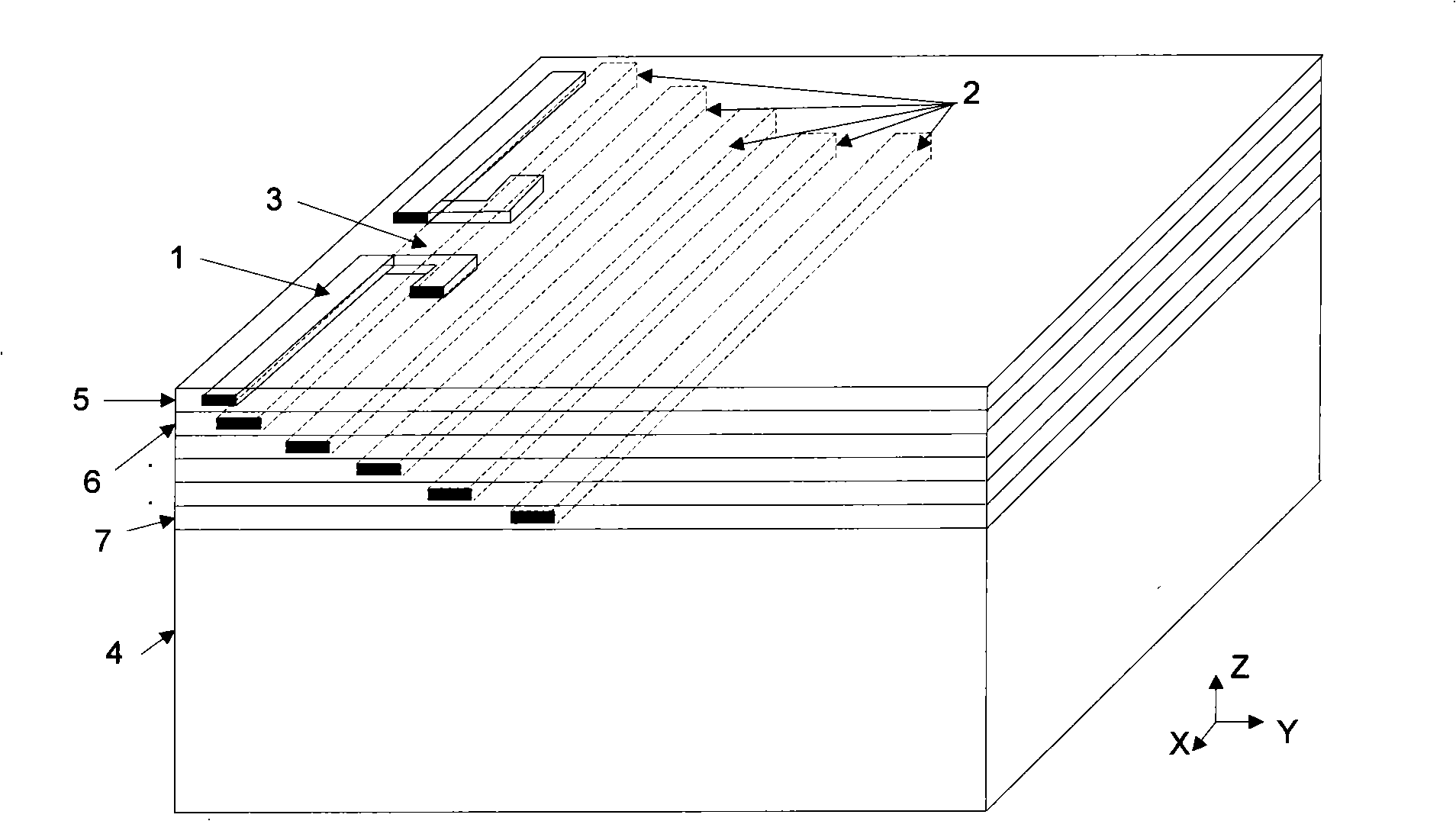
[0021] The structure of the ladder reflection directional chip antenna of the present invention is as follows: figure 1 As shown, it is located on a silicon substrate 4 and consists of an excitation pole 1 and several reflection poles 2 . The excitation pole 1 is located on the top metal layer 5 of the chip and is close to the edge of the chip. Several reflection poles 2 are located on the first metal layer 6 to the nth metal layer 7 sequentially from below the top metal layer 5, and are arranged in steps, each There is at most one reflector 2 in the layer metal layer. Here, n is the number of metal layers in the processing technology-1.

[0022] In the present invention, the quantity, length and spacing of the reflectors are variable and determined according to the gain and direction coefficient required by the design.
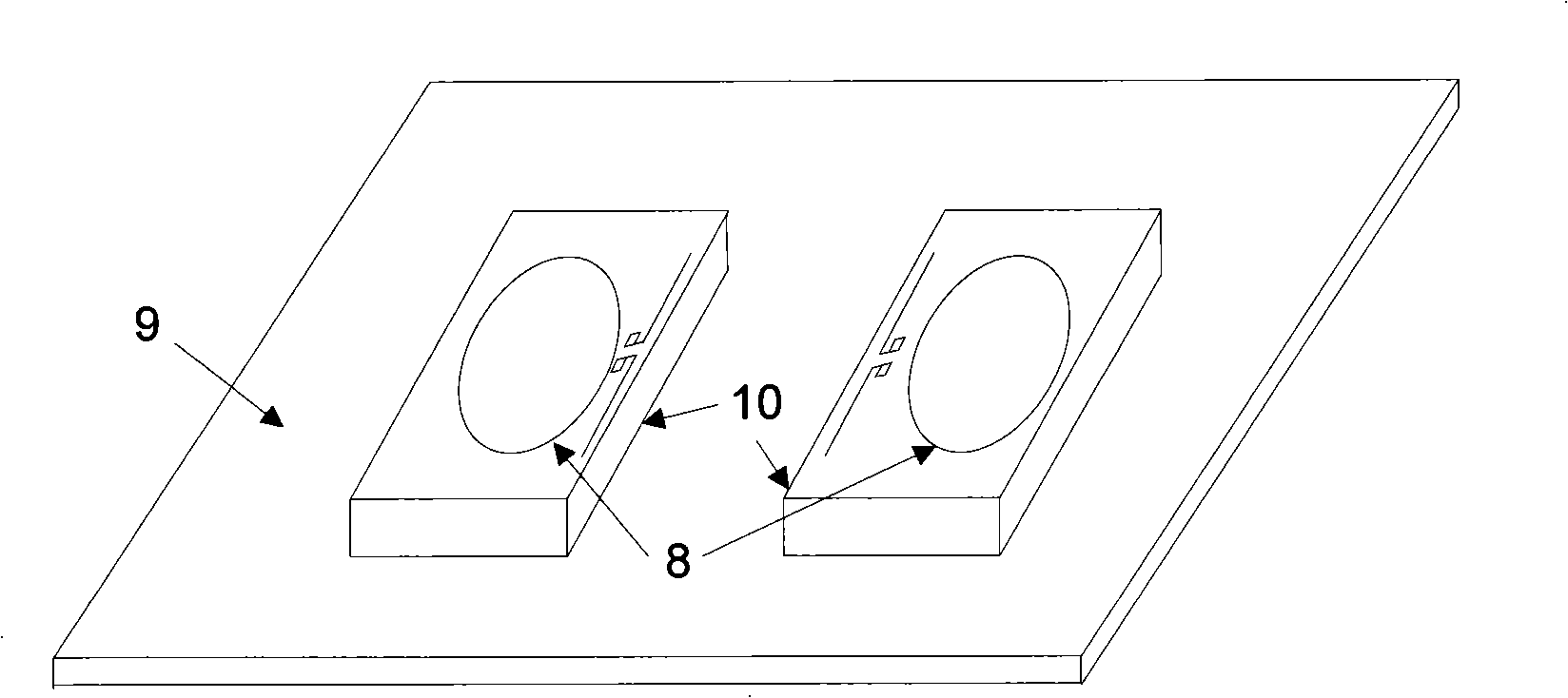
[0023] figure 2 ...


PUM

PropertyMeasurementUnit
Arm widthaaaaaaaaaa
Lengthaaaaaaaaaa
Arm widthaaaaaaaaaa

Abstract

This invention refers to an antenna on an echelon reflection positioning sheet applied to wireless interconnection among chips, belonging to the electronic technical field. The design theory of the antenna is rooted from Yagi aerial and just includes an excitation polaron and a reflection polaron without a positioning polaron in order to reduce the antenna area; according to the internal structure feature of the chip, the antenna is placed at the part close to the chip edge; the excitation plaron is located at a top metal layer of the chip; a plurality of reflection polaron is located at the metal layer under the top metal layer and is arranged in echelon. This invention with compact structure is able to generate the on-chip antenna ordered by different gains and direction coefficients through adjusting the arm width of each polaron, the number, length and gap of the reflection polaron; small taking area and simple structure of the antenna are easily to be achieved by adopting the standard CMOS technique.

Description

technical field [0001] The invention relates to a stepped reflective directional on-chip antenna, which is a stepped reflective directional on-chip antenna applied to wireless interconnection between chips, and belongs to the field of electronic technology. Background technique [0002] With the continuous development and improvement of modern technology, the grid pitch of MOS tubes is getting smaller and smaller, and the rate supported by CMOS chips can reach 40GHz. Chips on the same PCB (printed circuit board) are generally interconnected by metal interconnection wires. As the frequency continues to rise, the problems of parasitic resistance, parasitic capacitance and parasitic inductance of traditional metal interconnection wires become more and more serious, and the resulting RC delay hours, IR drop, CV 2 f Power consumption and crosstalk between lines will become bottlenecks restricting the development of high-speed circuits and radio frequency circuits. At the same t...

Claims


Application Information

Patent Timeline
IPC IPC(8): H01Q1/22H01Q1/38H01Q3/24
Inventor 江波涛毛军发李征帆尹文言金荣洪
Owner SHANGHAI JIAO TONG UNIV
Why Eureka
Try Eureka