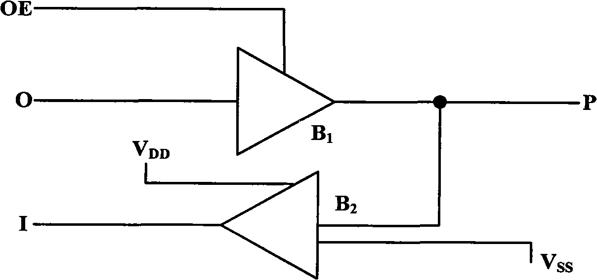
Input/output circuit and input control circuit

A control circuit and output terminal technology, applied in the direction of logic circuit connection/interface layout, logic circuit coupling/interface using field effect transistors, etc., can solve power loss, shorten the battery life of portable consumer electronics products, and improve the power consumption of portable consumer electronics products. Battery and other issues

Inactive Publication Date: 2008-12-17
ACTIONS ZHUHAI TECH CO
View PDF0 Cites 2 Cited by
  • Summary
  • Abstract
  • Description
  • Claims
  • Application Information

AI Technical Summary

Problems solved by technology

[0012] resulting in a V DD and V SS There is a loss of electrical energy between them, resulting in energy loss when the P point is suspended
[0013] In addition, when OE is high potential and this I / O circuit is used for output, the potential change of the output terminal O will pass through the input control circuit B 2 Passing to the input terminal I will cause the circuit connected to the input terminal I to be disturbed by the output signal, and also cause power loss because the circuit connected to the input terminal is disturbed; and the I / O circuit structure in the prior art will also be When used as a signal output, it will interfere with the circuit connected to the input terminal
[0014] Due to the extensive use of I / O circuits in chips, the power loss of I / O circuits in the prior art based on the above reasons will greatly increase the power consumption of portable consumer electronics products, thereby shortening the battery life of portable consumer electronics products.

Method used


Image

  • Input/output circuit and input control circuit
  • Input/output circuit and input control circuit
  • Input/output circuit and input control circuit

Examples


Embodiment Construction

[0068] The embodiment of the present invention provides an input control circuit, an input circuit and an input / output circuit (hereinafter referred to as I / O circuit) that can be used in integrated circuits. energy loss, so as to achieve the purpose of saving electric energy and improving the battery life of portable consumer electronic products; at the same time, the I / O circuit provided in the embodiment of the present invention can also reduce the interference of the output signal to the input terminal when the circuit is used for output, and at the same time Reduce the power loss of the input circuit due to interference.

[0069] image 3 is a circuit diagram of the input control circuit provided by the embodiment of the present invention, such as image 3 shown, the input control circuit B 3 Including: two PMOS transistors P 31 and P 32 , and two NMOS transistors N 31 and N 32 , V DD connected to the power supply, P 31 and P 32 The source potential is high, V S...


PUM


Abstract

The invention relates to an input control circuit in an integrated circuit, an input circuit and an input / output circuit, wherein the input / output circuit comprises a pin, an input end, a power input end and input control circuit, which includes a first PMOS pipe, a second PMOS pipe, an NMOS pipe, an input enable end and an input enable inverter. The source of the first PMOS pipe is connected with the input end of the power; the grid of the first PMOS pipe and the grid of the NMOS pipe are respectively connected with the input enable end; the drain of the first PMOS pipe, the source of the second PMOS pipe and the drain of the NMOS pipe are respectively connected with the input enable inverter; the drain of the second PMOS pipe and the source of the NMOS pipe are respectively connected with the pin P.

Description

technical field [0001] The invention relates to an integrated circuit, in particular to an input / output circuit and an input control circuit. Background technique [0002] In recent years, portable consumer electronic products have achieved considerable development, and are gradually replacing traditional electronic products as the first choice for people's consumption. Due to the particularity of portable consumer electronics products, an important performance indicator of such electronic products is the continuous working time after charging, that is, the battery life. For many users, the battery life is the decisive factor to measure whether a product is worth buying. one of the factors. [0003] The input / output circuit of the integrated circuit chip (hereinafter referred to as the I / O circuit) is the interface for data exchange between the integrated circuit chip and the external circuit. It is a circuit that can be used for both input and output. I / O circuits are wid...

Claims


Application Information

Patent Timeline
Patent Type & AuthorityApplications(China)
IPC IPC(8): H03K19/0185
Inventor易满星何再生王惠刚
OwnerACTIONS ZHUHAI TECH CO