Curved surface composite super resolution current-carrying tube

A super-resolution, curved surface technology, applied in the analysis of materials, surface/boundary effects, measurement devices, etc., can solve the problems of failure to achieve super-resolution detection of biological and metal micro-nano structures, limited application range, incomplete accuracy, etc. Filtering characteristics and anti-interference, simple and easy to use, the effect of avoiding errors

Inactive Publication Date: 2008-12-24
UNIV OF SCI & TECH OF CHINA
View PDF0 Cites 7 Cited by
  • Summary
  • Abstract
  • Description
  • Claims
  • Application Information

AI Technical Summary

Problems solved by technology

However, the near-field optical microscope restricts the fiber probe to work in the near field (several to tens of nanometers), requires a very sophisticated control system, and the operation is complicated and requires great care. The fiber probe must also be replaced regularly, requiring professional technicians, while also expensive, limiting its scope of application
Moreover, compared with the far-field detection that does not change the incident light field, the near-field detection destroys the analyzed light field, which will introduce errors and is not completely accurate
[0004] In 2007, Zhang Xiang et al. from the University of California, Berkeley used the metal-dielectric multilayer composite cylindrical structure to realize the principle experiment of far-field magnified imaging of micro-nano characters etched on the chromium metal layer, but did not realize Super-resolution detection of biological and metal micro-nano structures

Method used


Image

  • Curved surface composite super resolution current-carrying tube
  • Curved surface composite super resolution current-carrying tube
  • Curved surface composite super resolution current-carrying tube

Examples


Embodiment 1

[0041] Embodiment 1: The sample 6 to be tested in this embodiment is a fluorescently stained biological sample.

[0042] A hollow curved surface carrier is used, and at least one metal layer and a dielectric layer are arranged alternately to form a composite structure. The metal-dielectric multilayer composite curved surface structure needs to be constructed as a spherical geometry or a cylindrical geometry, so as to effectively prevent light from passing through different distances. The phase difference caused by different attenuation. The sample to be tested is placed in the cavity.

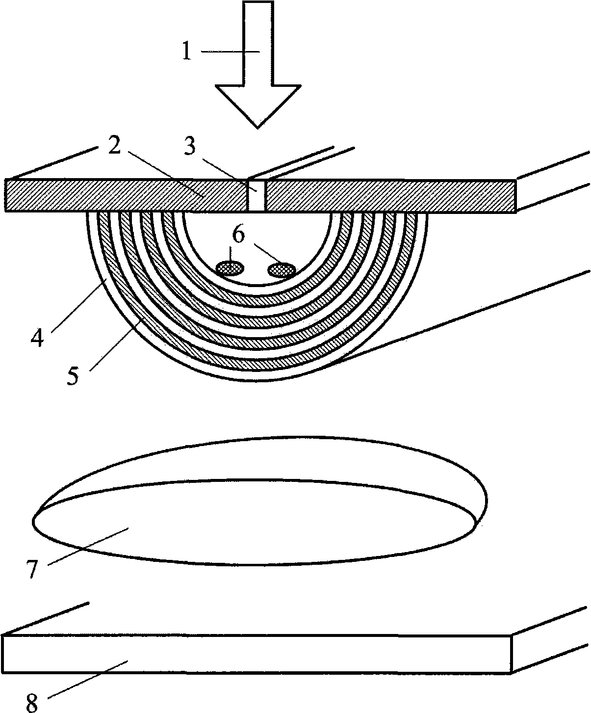
[0043] see figure 1 , in this embodiment, the curved surface carrier is a hollow semi-cylindrical body formed along the axial section, and the section is covered with a light-shielding layer 2 .

[0044] The light-shielding layer 2 selects chromium Cr with a thickness of 50nm, or other media with a transmittance of 0; on the light-shielding layer 2, a 50nm-wide light-transmitting slit 3 is op...

Embodiment 2

[0049] Embodiment 2: In this embodiment, the sample 6 to be tested is a metal nanoparticle sample.

[0050] The structure of the current-carrying tube is the same as above, see figure 1 . In this embodiment, the curved surface carrier is a hollow semi-cylindrical body formed along the axial section, and the section is covered with the light-shielding layer 2 . The light-shielding layer 2 selects chromium Cr with a thickness of 50nm, or other media with a transmittance of 0; on the light-shielding layer 2, a 50nm-wide light-transmitting slit 3 is opened along the axial direction of the semi-cylindrical body. This structure is to shield the light beam. Avoid irradiating the excitation light directly onto the imaging screen, which will affect the observation.

[0051] The light-transmitting slit 3 is located at the central axis of the current-carrying tube, and the irradiating light 1 can only enter the current-carrying tube from the slit, which is equivalent to a line light so...


PUM

PropertyMeasurementUnit
thicknessaaaaaaaaaa
thicknessaaaaaaaaaa
thicknessaaaaaaaaaa

Abstract

The invention provides a curved-surface composite super-resolution current-carrying pipe which is characterized in that a hollow curved-surface current carrier is adopted; the curved-surface current carrier is a composite structure which is formed by at least a metal layer and a dielectric layer, the sample to be tested is arranged in the hollow chamber thereof. The curved-surface composite super-resolution current-carrying pipe leads the dielectric constants in the normal direction and tangential direction to have opposite symbols by constructing the curved-surface composite structure of metal and dielectric and leads high frequency quantity which carries fine structure information and can not be transmitted in normal lens to be transmitted in the curved-surface composite super-resolution current carrying pipe wall and not to generate mutual interference; the dot pitch is more than the Rayleigh resolution limit when the high frequency quantity is emitted out through the curved surface of the external wall of the current carrying pipe, thus realizing that the sample structure of nanometer-class exceeding the diffraction resolution limit can be observed far away; the curved-surface composite super-resolution current-carrying pipe has high resolution, avoids the error of close detection and has far imaging which is more convenient for operation and application.

Description

technical field [0001] The invention relates to optical microscopic imaging technology, in particular to a detection device capable of realizing far-field magnified imaging beyond the Rayleigh resolution limit for nanoscale samples. Background technique [0002] Generally, optical observation instruments working in the far field (much longer than one wavelength) cannot avoid the interference and diffraction effects caused by the fluctuation of light. Limited by the Rayleigh resolution limit, for example, when using light with a wavelength of λ, all current far-field lenses cannot magnify and resolve two samples separated by a distance less than λ / 2. [0003] In 1984, D. Pohl and others from IBM in Zurich, Switzerland used microapertures as microprobes to make the world's first near-field optical microscope. Two years later, E. Betzig of Cornell University in the United States also made a near-field optical microscope using a micropipette as a probe. Subsequently, various n...

Claims


Application Information

Patent Timeline
Patent Type & Authority Applications(China)
IPC IPC(8): G01N13/10G01Q30/20
Inventor 曹勇王沛鲁拥华明海
Owner UNIV OF SCI & TECH OF CHINA
Why Eureka
Try Eureka