Single-phase control node apparatus of wireless sensor network
A wireless sensor and network technology, applied in the direction of comprehensive factory control, comprehensive factory control, electrical program control, etc., can solve problems such as unseen, and achieve the effect of convenient use and maintenance, good real-time performance, and convenient maintenance.
- Summary
- Abstract
- Description
- Claims
- Application Information
AI Technical Summary
Problems solved by technology
Method used
Image
Examples
Embodiment 1
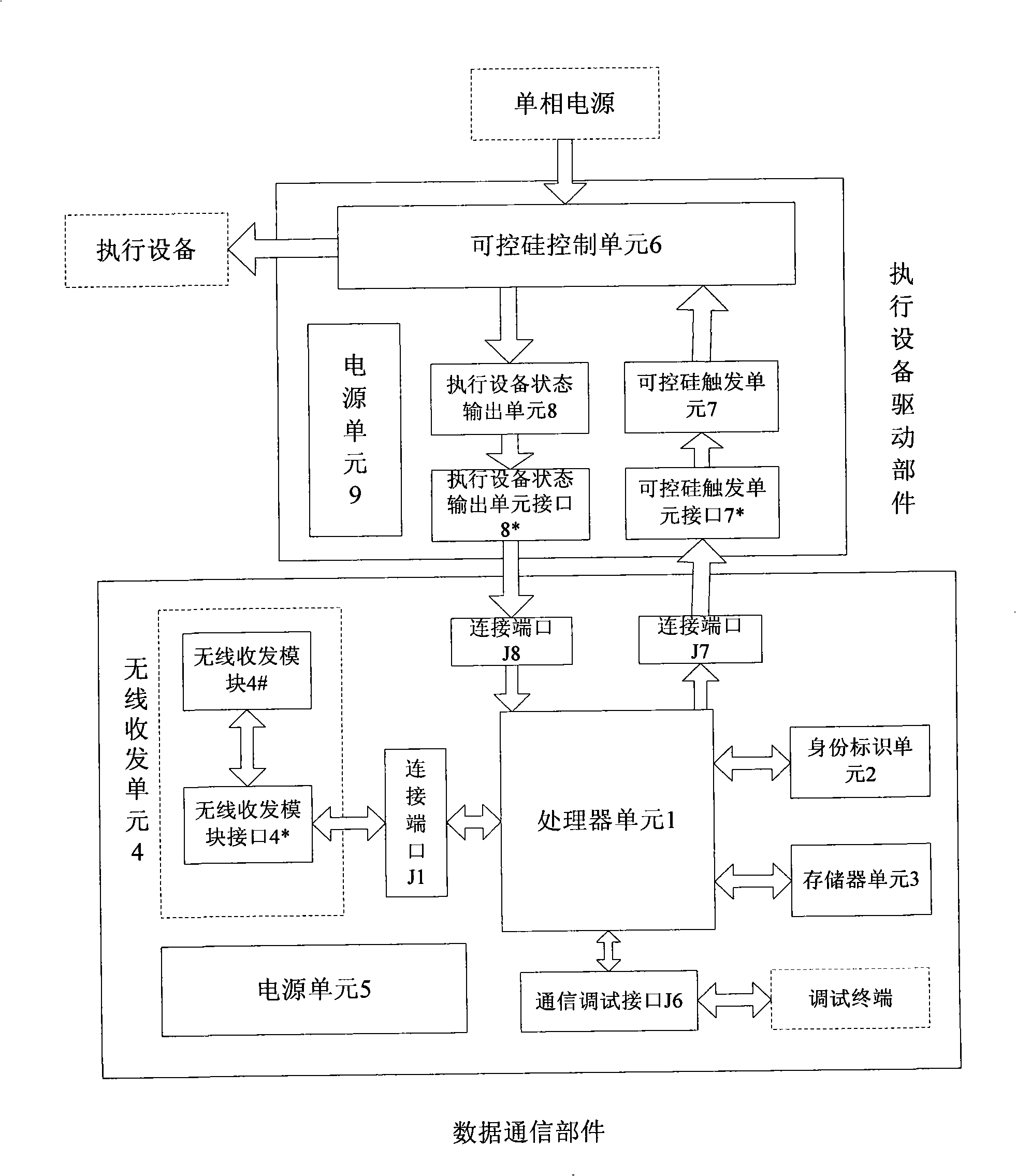
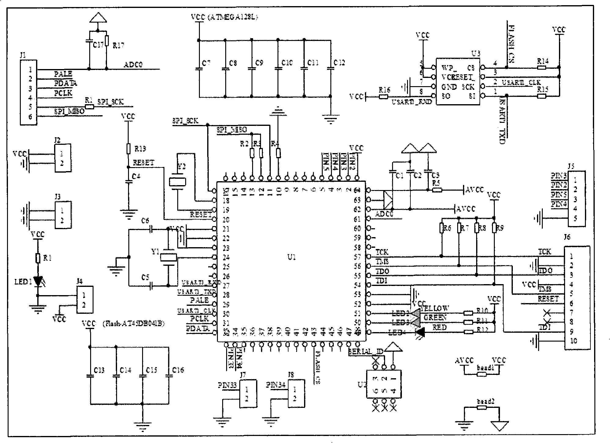
[0055] An implementation example of the above-mentioned data communication components (not including the power supply unit 5 and the wireless transceiver unit 4) can be seen image 3 . It is mainly composed of processor unit 1, identity identification unit 2, memory unit 3, connection ports J1, J2, J3 connected to wireless transceiver module interface 3*, power supply unit interface J4, communication debugging interface J6, connection port J7, connection port J8 composition.
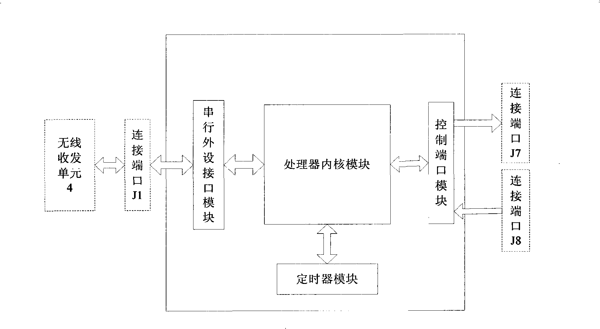
[0056] The microprocessor chip U1 in the processor unit 1 selects the high-performance, low-power AVR 8-bit high-end microprocessor ATmegal28L of AT Company. It has an advanced RISC structure, the highest operating frequency is 8MHz, most instructions are completed in one cycle, and the operation rate is high; on-chip 128kFlash, 4kSRAM and 4kEEPROM; supports 6 sleep modes such as power-saving mode and power-down mode; has a variety of Bus and sufficient input and output interfaces; with A / D, D / A interf...
Embodiment 2
[0066] According to the selected chip and connection mode of Embodiment 1, the flow process of the functions realized by the microprocessor chip U1 in the processor unit 1 of the above-mentioned data communication component is as follows Figure 6 As shown, it includes:
[0067] Step 1: The processor core module completes initialization tasks, including initialization of internal memory and registers, initialization of I / O ports, initialization of potentiometers, initialization of scheduler, initialization of application program components, and opening of interrupts. The processor core module clears the zeroth bit of the G port data register to 0, and outputs a TTL low level to PG0. Simultaneously start the time synchronization timer to start counting.
[0068] Step 2 The processor core module processes the data packet received by the serial device interface module.
[0069] 1) If the address of the received data packet is the ID number of the node device, the length is CONT...
Embodiment 3
[0079] An implementation example of the execution device driver component can be seen in Figure 7 , which is mainly composed of thyristor control unit 6, thyristor trigger unit 7, thyristor trigger unit interface 7*, execution device state output unit 8, execution device state output unit interface 8*, and power supply unit 9. The "PIN33" pin of the thyristor trigger unit interface 7* is connected to the "33" pin of the microprocessor chip U1 through the connection port J7; the "PIN34" pin of the output unit interface 8* of the execution device is connected to the The "34" pin of the microprocessor chip U1 is connected.
[0080] In the thyristor control unit 6, the thyristor Q2 placed in the AC main circuit is selected from BTA26BW, and the maximum allowable passing current is 26A, which can meet the requirements of most applications.
[0081] In the thyristor trigger unit 7, the triode Q1 is a general-purpose semiconductor device 8050, the emitter of Q1 is connected to the ...
PUM
 Abstract
Description
Claims
Application Information


