Last-first mode and method for programming of non-volatile memory of NAND type with reduced program disturb

A non-volatile storage and programming interference technology, applied in static memory, read-only memory, digital memory information, etc.

Inactive Publication Date: 2009-01-28
SANDISK TECH LLC
View PDF14 Cites 14 Cited by
  • Summary
  • Abstract
  • Description
  • Claims
  • Application Information

AI Technical Summary

Problems solved by technology

However, one memory element in each NAND string uses the same word line, and thus will experience the programming voltage

Method used


Image

  • Last-first mode and method for programming of non-volatile memory of NAND type with reduced program disturb
  • Last-first mode and method for programming of non-volatile memory of NAND type with reduced program disturb
  • Last-first mode and method for programming of non-volatile memory of NAND type with reduced program disturb

Examples


Embodiment Construction

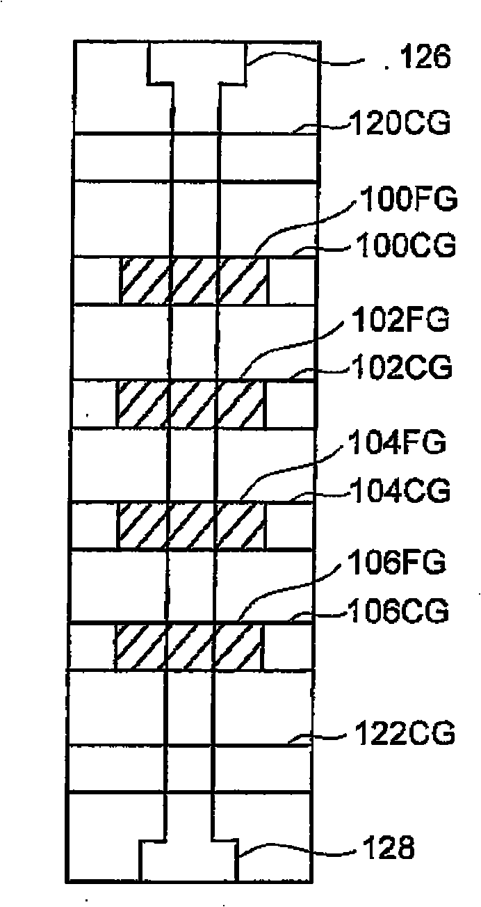
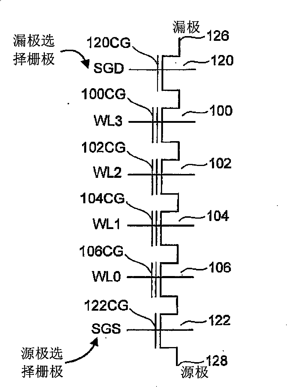
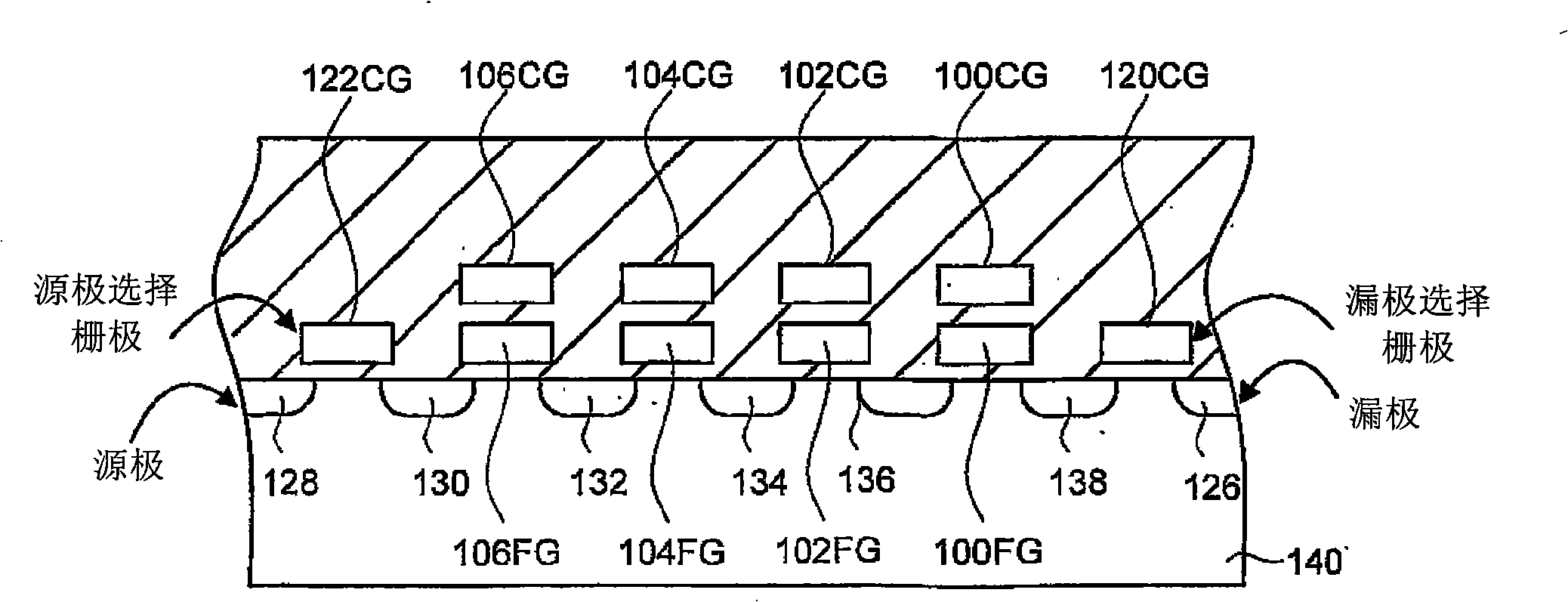
[0033] One example of a non-volatile memory system suitable for implementing the present invention uses a NAND flash memory structure in which multiple transistors are arranged consecutively between two select gates of a NAND string. figure 1 is a top view showing a NAND string. figure 2 is its equivalent circuit diagram. figure 1 and 2The NAND string depicted in includes four transistors 100 , 102 , 104 , and 106 sandwiched in series between a first select gate 120 and a second select gate 122 . Select gates 120 and 122 connect the NAND string to bit line contact 126 and source line contact 128, respectively. Select gates 120 and 122 are controlled by applying appropriate voltages to control gates 120CG and 122CG. Each of the transistors 100, 102, 104, and 106 has a control gate and a floating gate. The transistor 100 has a control gate 100CG and a floating gate 100FG. Transistor 102 includes control gate 102CG and floating gate 102FG. Transistor 104 includes control g...


PUM


Abstract

A non-volatile memory is programmed in a manner which reduces the incidence of program disturb for inhibited memory elements which undergo boosting to reduce program disturb, but which experience reduced boosting benefits due to their word line location. To achieve this result, a word line sequence in which the memory elements are programmed is adjusted so that higher word lines are programmed first, out of sequence relative to the remaining word lines. Additionally, self-boosting can be used for the higher word lines, while erased area self-boosting or a variant can be used for the remaining word lines. Furthermore, pre-charging of the channel of the inhibited memory elements may be employed prior to the self boosting, for the non-volatile storage elements which are programmed after those associated with the first word line.

Description

technical field [0001] The present invention relates to programming non-volatile memory. Background technique [0002] Semiconductor memories have become more and more commonly used in various electronic devices. For example, non-volatile semiconductor memory is used in cellular telephones, digital cameras, personal digital assistants, mobile computing devices, non-mobile computing devices, and other devices. Electrically Erasable Programmable Read Only Memory (EEPROM) and flash memory are among the most popular non-volatile semiconductor memories. In contrast to conventional full-featured EEPROMs, flash memory (which is also a type of EEPROM) can erase the contents of the entire memory array or a portion of the memory in one step. [0003] Both traditional EEPROM and flash memory use a floating gate that is located above and isolated from a channel region in a semiconductor substrate. The floating gate is located between the source region and the drain region. The contr...

Claims


Application Information

Patent Timeline
Patent Type & Authority Applications(China)
IPC IPC(8): G11C16/04
CPCG11C16/349G11C16/0483G11C16/3418G11C2211/5648G11C11/5628
Inventor 万钧杰弗里·W·卢策
Owner SANDISK TECH LLC
Why Eureka
Try Eureka