Flash memory and manufacturing method thereof

A manufacturing method and flash memory technology, which can be applied to electrical components, electrical solid devices, circuits, etc., can solve problems such as unfavorable and unfavorable component erasing operations, and achieve improved performance, improved memory data retention, and elimination of memory cell dislocations. Effect

Active Publication Date: 2011-12-28
MACRONIX INT CO LTD
View PDF0 Cites 0 Cited by
  • Summary
  • Abstract
  • Description
  • Claims
  • Application Information

AI Technical Summary

Problems solved by technology

[0006] However, if Figure 1B As shown, after the annealing process 116, whether it is the edge thickness t of the tunnel oxide layer 102 or the inter-gate dielectric layer 106 edge both become thicker than their central thickness t center Thick, so it is not conducive to the control of the gate coupling ratio (gate coupling ratio, GCR) between the charge storage layer and the control gate, which affects the operating voltage and device speed
Moreover, when the flash memory performs an erase operation, the area between the tunnel oxide layer 102 and the channel (that is, the area between the source electrode 118a and the drain electrode 118b) is related, so when the edge of the tunnel oxide layer 102 When thickened, it will not be conducive to the erasing operation of the component

Method used


Image

  • Flash memory and manufacturing method thereof
  • Flash memory and manufacturing method thereof
  • Flash memory and manufacturing method thereof

Examples


Embodiment Construction

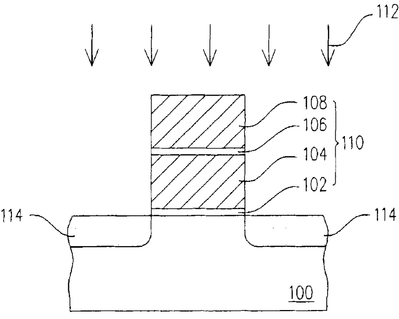
[0051] Figure 2A to Figure 2E is a sectional view of a manufacturing process of a flash memory according to an embodiment of the present invention.

[0052] Please refer to Figure 2A , forming a stack structure 210 on the substrate 200, for example, the stack structure 210 includes a tunnel oxide layer 202, a charge storage layer 204, an intergate dielectric layer 206 and a layer Control grid 208 . Wherein, the material of the charge storage layer 204 is, for example, doped polysilicon, silicon nitride or other materials capable of storing charges. The tunnel oxide layer 202 and the inter-gate dielectric layer 206 are, for example, one of materials selected from oxide layers, nitride layers, nitride and oxide layers, oxide, nitride and oxide layers. The material of the control gate 208 is, for example, selected from one of materials composed of doped polysilicon, metal silicide, and conductive metal. In addition, the stack structure 210 may include other film layers, suc...


PUM


Abstract

Disclosed is a flash memory, comprising a substrate, a stack structure arranged on the substrate, a source electrode, a drain electrode and a source terminal spacing layer; wherein the stack structure is composed of a tunnel oxide layer, a charge storage layer arranged on the tunnel oxide layer, an inter-gate medium layer arranged on the charge storage layer and a control grid arranged on the inter-gate medium layer. The source electrode and the drain electrode are arranged in the substrate respectively at two sides of the charge storage layer. The source terminal spacing layer is arranged on one side wall of the stack structure, which is close to the source electrode, so as to prevent the parts of the tunnel oxide layer and the inter-gate medium layer, which are close to the source electrode, from being oxidated again, which leads to the increase of the thickness.

Description

technical field [0001] The present invention relates to a non-volatile memory and its manufacturing method, and in particular to a flash memory with an asymmetric spacer layer structure and its manufacturing method. Background technique [0002] A typical flash memory uses doped polysilicon to make a charge storage layer and a control gate. When the memory is being programmed, appropriate programming voltages are applied to the source, drain and control gate respectively, and electrons will flow from the source to the drain through a channel. During this process, some electrons will pass through the tunneling oxide layer under the polysilicon charge storage layer, enter and be evenly distributed in the entire polysilicon charge storage layer, such electrons pass through the tunneling oxide layer The phenomenon of entering the polysilicon charge storage layer is called tunneling effect. The tunneling effect can be divided into two cases, one is called channel hot-electron i...

Claims


Application Information

Patent Timeline
Patent Type & Authority Patents(China)
IPC IPC(8): H01L29/792H01L29/423H01L27/115H01L27/11521H01L27/11531
Inventor 易成名
Owner MACRONIX INT CO LTD
Why Eureka
Try Eureka