Organic thin-film transistor and manufacture method thereof
A technology of organic thin film and transistor, which is applied in the field of organic thin film transistor and its preparation, can solve the disadvantages of large-scale production of organic thin film transistor, etc., and achieve the effects of easy tailoring and processing, improved performance and novel structure
- Summary
- Abstract
- Description
- Claims
- Application Information
AI Technical Summary
Problems solved by technology
Method used
Image

Examples
Embodiment 1
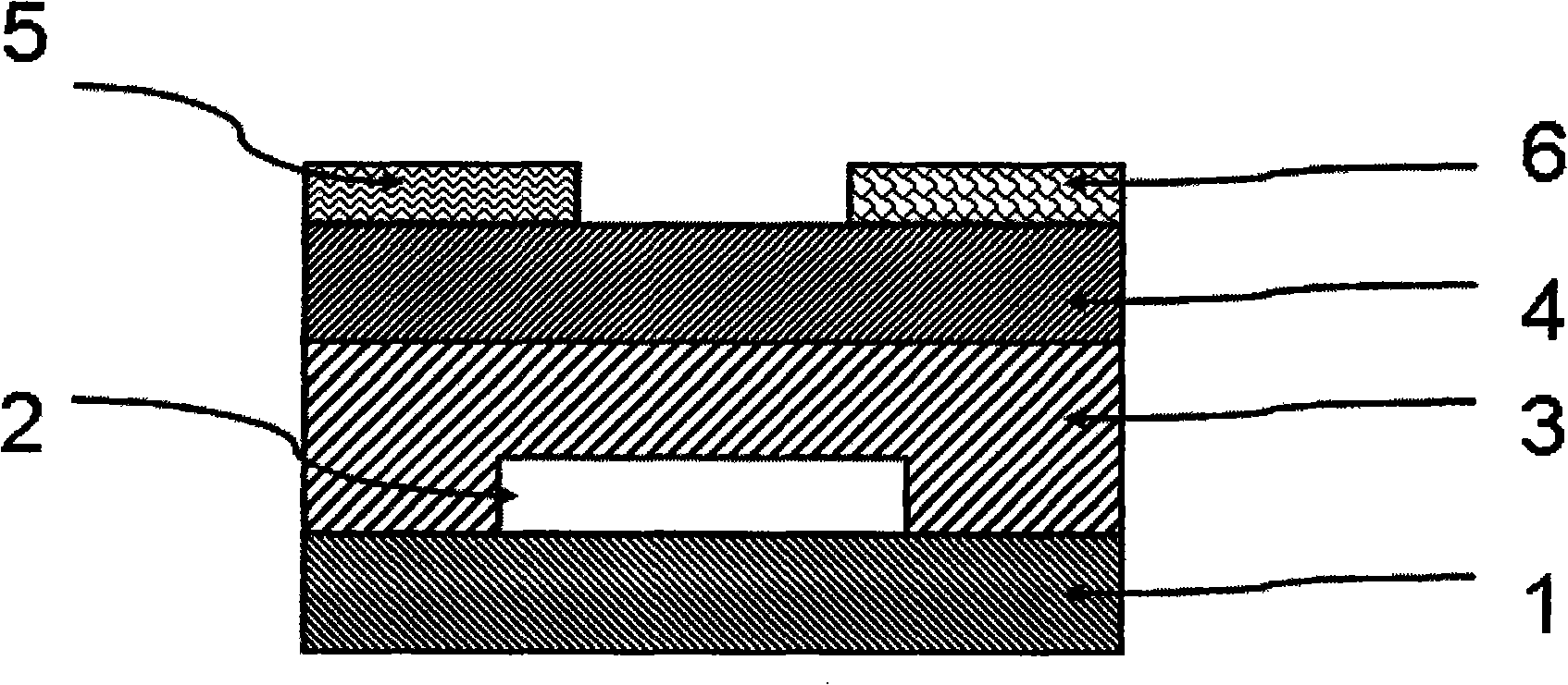
[0046] Such as figure 1 In the structure shown, substrate 1 is made of Si substrate, gate electrode 2 is made of DC magnetron sputtered ITO transparent conductive film, ultraviolet curing adhesive is used as organic gate insulating layer 3, source electrode 5 is made of Cr metal film as electrode layer, and leakage current Electrode 6 also uses Cr metal thin film as an electrode layer, and organic semiconductor layer 4 uses pentacene pentance.
[0047] The preparation method is as follows:
[0048] ① Thoroughly clean the Si substrate first, and blow dry with dry nitrogen after cleaning;
[0049] ② Evaporate the gate electrode on the surface of the Si substrate by DC magnetron sputtering;
[0050] ③Etching the ITO gate electrode pattern by photolithography;
[0051] ④ On the Si substrate plated with the gate electrode, spin-coat the UV-curable adhesive organic gate insulating layer by spin-coating;
[0052] ⑤ Carrying out ultraviolet curing and heating and baking the formed...
Embodiment 2
[0057] Such as figure 1 In the structure shown, substrate 1 is made of Si substrate, gate electrode 2 is made of DC magnetron sputtered ITO transparent conductive film, ultraviolet curing adhesive is used as organic gate insulating layer 3, source electrode 5 is made of Cr metal film as electrode layer, and leakage current The electrode 6 also adopts Cr metal thin film as an electrode layer, and the organic semiconductor layer 4 adopts CuPc.
[0058] The fabrication process of the device is similar to that of Example 1.
Embodiment 3
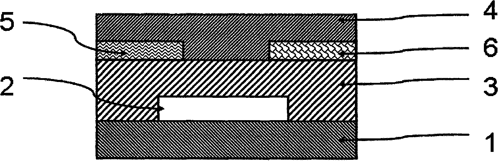
[0060] Such as figure 2 In the structure shown, substrate 1 is made of Si substrate, gate electrode 2 is made of DC magnetron sputtered ITO transparent conductive film, ultraviolet curing adhesive is used as organic gate insulating layer 3, source electrode 5 is made of Cr metal film as electrode layer, and leakage current The electrode 6 also uses Cr metal thin film as the electrode layer, and the organic semiconductor layer 4 uses pentacene.
[0061] The preparation method is as follows:
[0062] ① Thoroughly clean the Si substrate first, and blow dry with dry nitrogen after cleaning;
[0063] ② Evaporate the gate electrode on the surface of the Si substrate by DC magnetron sputtering;
[0064] ③Etching the ITO gate electrode pattern by photolithography;
[0065] ④ On the Si substrate plated with the gate electrode, spin-coat the UV-curable adhesive organic gate insulating layer by spin-coating;
[0066] ⑤ Carrying out ultraviolet curing and heating and baking the forme...
PUM
| Property | Measurement | Unit |
|---|---|---|
| Thickness | aaaaa | aaaaa |
Abstract
Description
Claims
Application Information
 - R&D
- Intellectual Property
- Life Sciences
- Materials
- Tech Scout
- Unparalleled Data Quality
- Higher Quality Content
- 60% Fewer Hallucinations
Browse by: Latest US Patents, China's latest patents, Technical Efficacy Thesaurus, Application Domain, Technology Topic, Popular Technical Reports.
© 2025 PatSnap. All rights reserved.Legal|Privacy policy|Modern Slavery Act Transparency Statement|Sitemap|About US| Contact US: help@patsnap.com