

Organic opto-electronic device with composite protection layer and preparation method thereof
A technology for optoelectronic devices and protective layers, which is applied in the field of organic optoelectronic devices with composite protective layers and its preparation, can solve the problems of poor density and oxidation resistance of polymer packaging layers, insufficient smoothness of the surface, and low mechanical strength, etc., to achieve The effect of light weight, small size and reduced production cost
- Summary
- Abstract
- Description
- Claims
- Application Information
AI Technical Summary
Problems solved by technology
Method used
Image

Examples
Embodiment 1
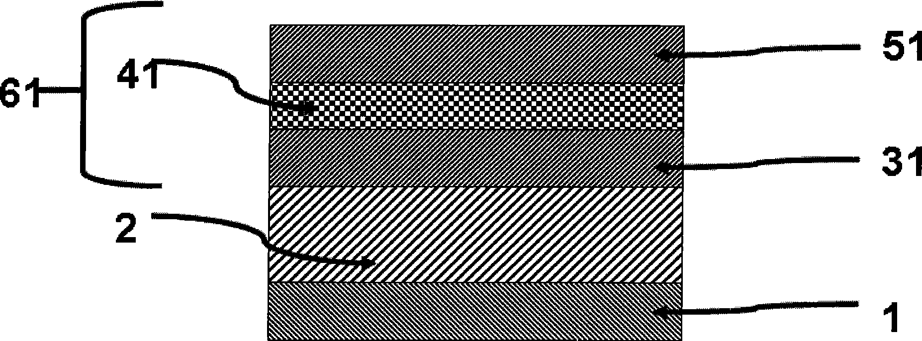
[0059] like figure 1 As shown, the substrate 1 in the structure of the device, the organic optoelectronic device 2 is an organic electroluminescence device, an organic material layer 31 , an organic material layer 41 , an inorganic material layer 51 , and a combination layer 61 .
[0060] The substrate 1 of the device is PET, an organic electroluminescent device, the inorganic material layer 31 is silicon nitride, the organic material layer 41 is UV glue, and the inorganic material layer 51 is silicon nitride.
[0061] The preparation method is as follows:
[0062] ① Prepare an inorganic material layer silicon nitride 300nm on the upper layer of the organic electroluminescent device;
[0063] ② Evaporate or spin-coat a layer of organic material layer UV glue 300nm on the above inorganic material layer silicon nitride;
[0064] ③ Deposit a layer of inorganic material layer silicon nitride 300nm on the above organic material layer UV glue;
[0065] ④ Repeat the above steps ① ...
Embodiment 2
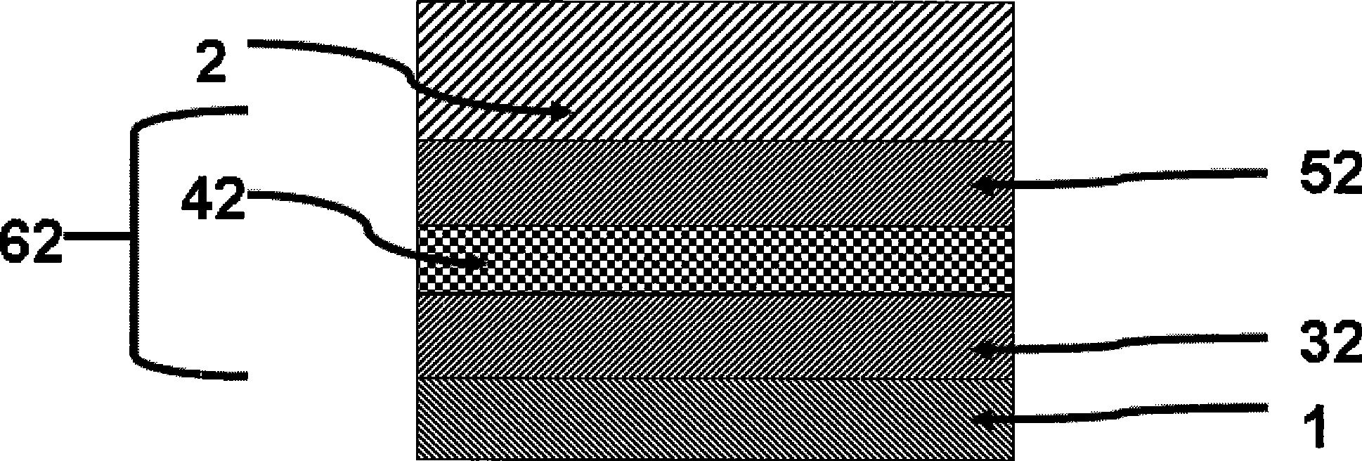
[0067] like figure 2 As shown, the substrate 1 in the structure of the device, the organic optoelectronic device 2 is an organic thin film transistor, an inorganic material layer 32 , an organic material layer 42 , an inorganic material layer 52 , and a combined layer 62 .
[0068] The substrate 1 of the device is PET, organic thin film transistor, the inorganic material layer 32 is silicon nitride, the organic material layer 42 is UV glue, and the inorganic material layer 52 is silicon nitride.
[0069] The fabrication process of the device is as follows:
[0070] ① Prepare an inorganic material layer silicon nitride 300nm on the upper layer of the substrate;
[0071] ② Prepare a layer of organic material layer UV glue 300nm on the above inorganic material layer silicon nitride;
[0072] ③ Deposit a layer of inorganic material layer silicon nitride 300nm on the above organic material layer UV glue;
[0073] ④Repeat the above steps ①~③, and then prepare a thin film layer c...
Embodiment 3
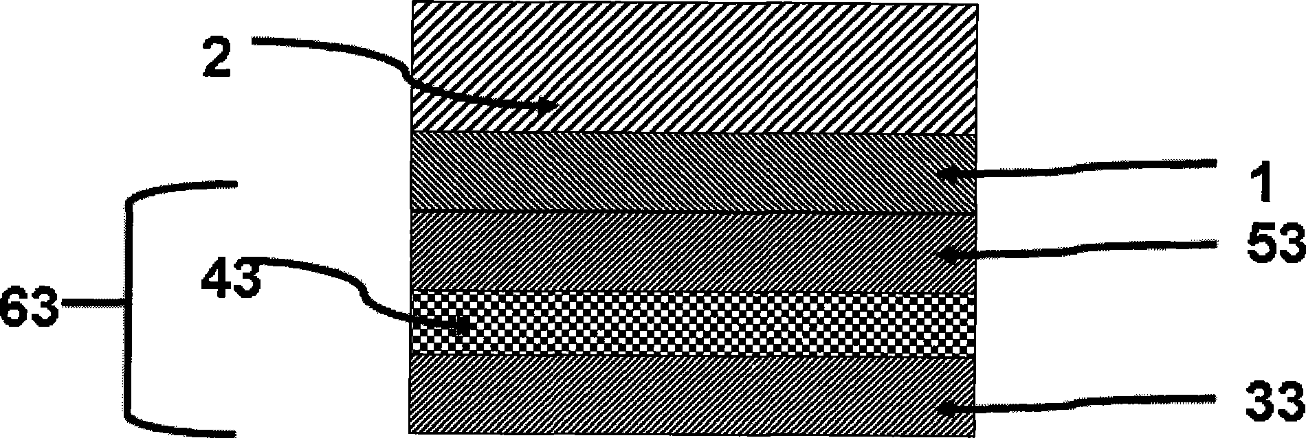
[0076] like image 3 As shown, the substrate 1 in the structure of the device, the organic optoelectronic device 2 is an organic solar cell, an inorganic material layer 33 , an organic material layer 43 , an inorganic material layer 53 , and a combination layer 63 .
[0077] The substrate 1 of the device is PET, an organic solar cell, the inorganic material layer 33 is silicon nitride, the organic material layer 43 is UV glue, and the inorganic material layer 53 is silicon nitride.
[0078] The fabrication process of the device is similar to that of Example 2.
PUM
 Abstract
Description
Claims
Application Information