SOI wafer manufacturing method and SOI wafer

一种制造方法、晶片的技术,应用在半导体/固态器件制造、电气元件、电固体器件等方向,能够解决晶片滑移位错、SOI晶片质量恶化等问题

Active Publication Date: 2012-05-16
SHIN-ETSU HANDOTAI CO LTD
View PDF3 Cites 0 Cited by
  • Summary
  • Abstract
  • Description
  • Claims
  • Application Information

AI Technical Summary

Problems solved by technology

[0010] However, in the above-mentioned method, when the epitaxial growth is performed at a high temperature on the SOI layer of the SOI wafer used as the substrate by using a lamp heating type epitaxial growth apparatus, slip dislocations and the like are likely to occur on the wafer. The quality deterioration of the problem points, there is still room for improvement

Method used


Image

  • SOI wafer manufacturing method and SOI wafer
  • SOI wafer manufacturing method and SOI wafer
  • SOI wafer manufacturing method and SOI wafer

Examples


Embodiment 1

[0069] Hereinafter, although the Example of this invention is illustrated and this invention is demonstrated more concretely, this invention is not limited to these Examples.

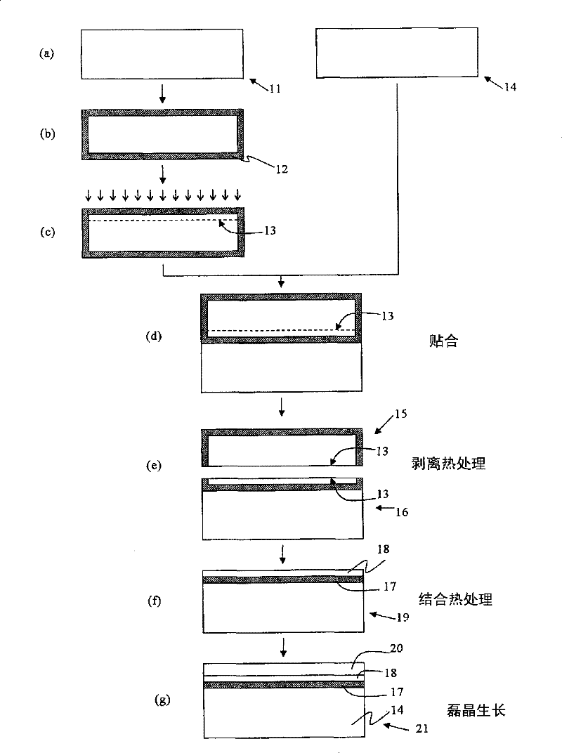
[0070] in accordance with figure 1 , a method of producing an SOI wafer serving as a substrate by an ion implantation lift-off method will be described.

[0071] Four thin disk-shaped wafers of CZ single crystal silicon substrates (diameter 200 mm (8 inches), thickness 625 μm) with an oxygen concentration of 20 ppma were prepared, and two were used as a bonding wafer and a base wafer.

[0072] Next, the two bonded wafers are heat-treated in an oxidizing environment to form an oxide film on the entire surface of the wafer. At this time, the time of the heat treatment was adjusted so that the thickness of the oxide film was 145 nm. For this bonded wafer, with a doping amount of 10×10 16 / cm 2 , and by adjusting the implantation energy to make the implantation depths of 195nm and 215nm, hydrogen ion im...

Embodiment 2

[0077] Embodiment 2, comparative example

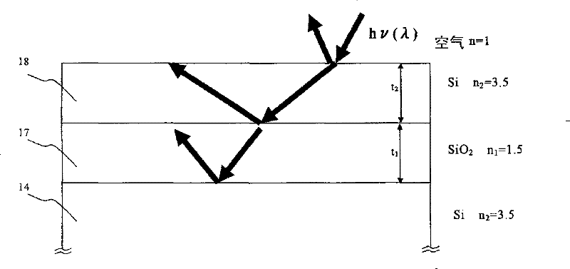
[0078] Next, seven SOI wafers serving as substrates were prepared by the same method as in Example 1 (implantation depth of 215 nm), and the thickness of the oxide film and the thickness of the SOI layer were adjusted so that the surface reflectances were respectively 30% to 95%. On these SOI wafers serving as substrates, an epitaxial layer of 1000 nm was grown under the conditions of a reaction temperature of 1050° C. and a reaction time of 30 seconds, thereby producing an SOI wafer.

[0079] The relationship between the total slip length measured after epitaxial growth and the reflectivity of the SOI wafer before epitaxial growth is shown in Figure 5 . In SOI wafers with a reflectivity of more than 80%, the total slip length may exceed the allowable value, that is, 100 mm. However, in SOI wafers with a reflectivity of less than 80%, the total slip length is below the allowable value. Almost zero below 70%. When the reflectance i...


PUM


Abstract

Provided is an SOI wafer manufacturing method for growing an epitaxial layer on an SOI layer of the SOI wafer obtained by forming an oxide film and an SOI layer on a base wafer so as to increase the SOI layer thickness. The epitaxial growth is performed in such a manner that the reflectance of the surface in a wavelength region of a heating light at the epitaxial growth start of the SOI wafer forgrowing the epitaxial layer is in the range from 30% to 80%. Thus, it is possible to provide a method for manufacturing an SOI wafer of high quality having a small slip shifting.

Description

technical field [0001] The present invention relates to a method for manufacturing an SOI wafer in which a semiconductor single crystal film is epitaxially grown on a silicon-on-insulator (SOI) wafer serving as a substrate, and the SOI layer is thickened. Background technique [0002] After bonding the bonding wafer and the base wafer, the bonding substrate obtained by thinning the bonding wafer is used as a semiconductor substrate for a high-performance device. As one of such bonded substrates, a silicon SOI substrate is known. [0003] As a manufacturing method of an SOI substrate, for example, the following bonding method is known. That is, two mirror-polished silicon wafers (the bonding wafer and the base wafer) are prepared first, and an oxide film is formed on at least one of the wafers. Then, after bonding these wafers with an oxide film interposed therebetween, the bonding strength is improved by heat treatment. After that, the bonded wafer is thinned to obtain an...

Claims


Application Information

Patent Timeline
Patent Type & Authority Patents(China)
IPC IPC(8): H01L21/02H01L21/20H01L21/205H01L27/12
CPCH01L21/76254H01L21/20
Inventor 八木真一郎
Owner SHIN-ETSU HANDOTAI CO LTD
Why Eureka
Try Eureka