Semiconductor device and a method for fabricating the same

A technology of semiconductors and devices, which is applied in the field of semiconductor devices and its manufacturing, can solve the problems of reducing the efficiency of inductors and the use of frequency bands, and achieve the effects of increasing effective values, expanding the available frequency range, and reducing parasitic capacitance

Inactive Publication Date: 2009-03-04
DONGBU HITEK CO LTD
View PDF0 Cites 0 Cited by
  • Summary
  • Abstract
  • Description
  • Claims
  • Application Information

AI Technical Summary

Problems solved by technology

[0007] As the parasitic capacitance increases, the efficiency and frequency band of the inductor decrease

Method used


Image

  • Semiconductor device and a method for fabricating the same
  • Semiconductor device and a method for fabricating the same
  • Semiconductor device and a method for fabricating the same

Examples


Embodiment Construction

[0018] When the terms "on" or "on" or "over" are used herein, where a layer, region, pattern or structure is referred to, it should be understood that said layer, region, pattern or structure may be directly on another layer or Structurally, or intervening layers, regions, patterns or structures may also be present. When the terms "beneath" or "beneath" are used herein, in reference to a layer, region, pattern or structure, it is to be understood that said layer, region, pattern or structure may be directly underlying another layer or structure, or also Intermediate layers, regions, patterns or structures may be present.

[0019] Reference will now be made in detail to embodiments of the invention, examples of which are illustrated in the accompanying drawings.

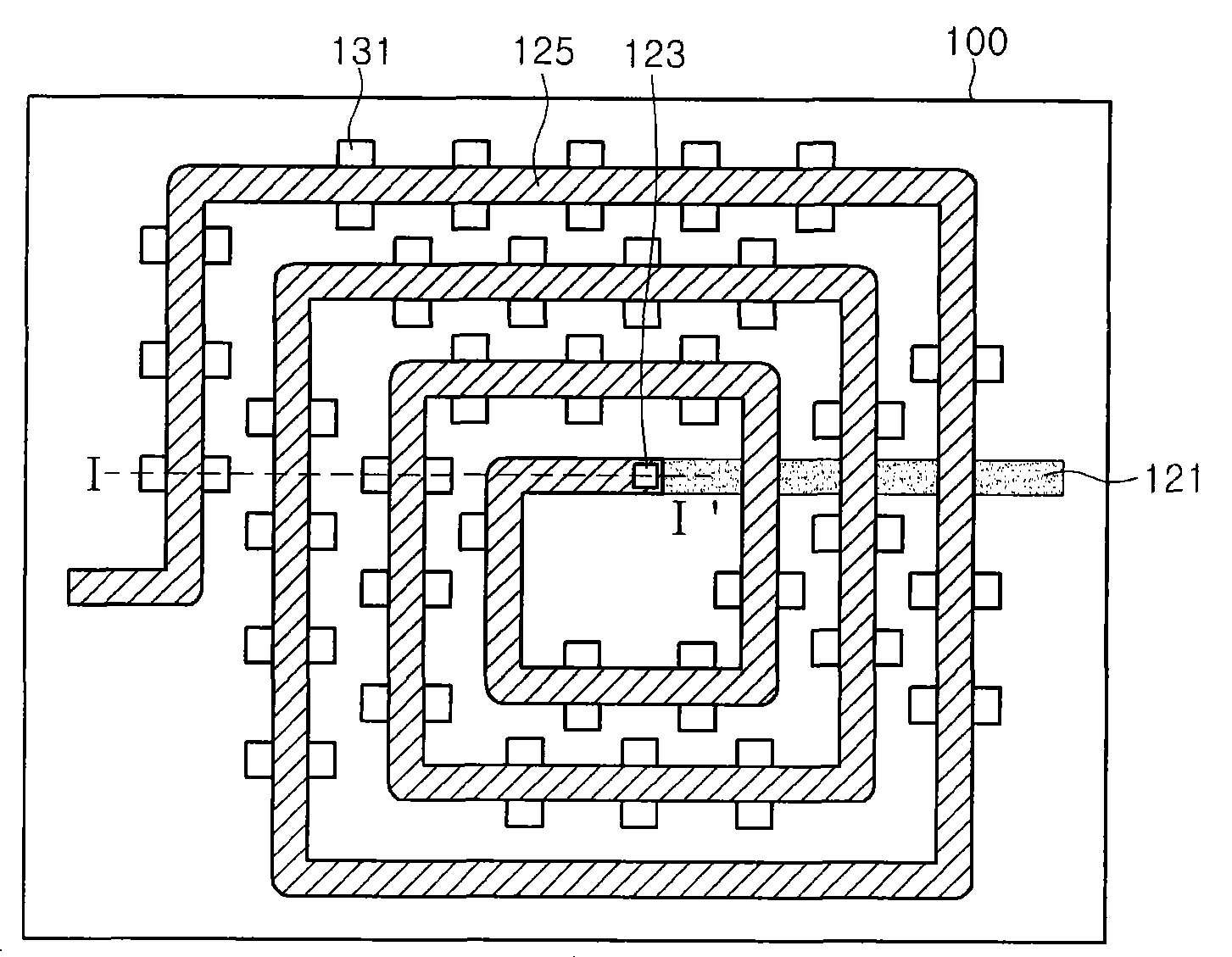
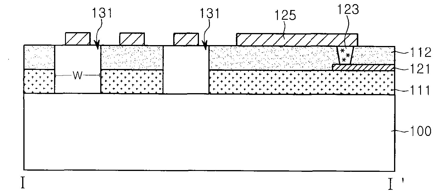
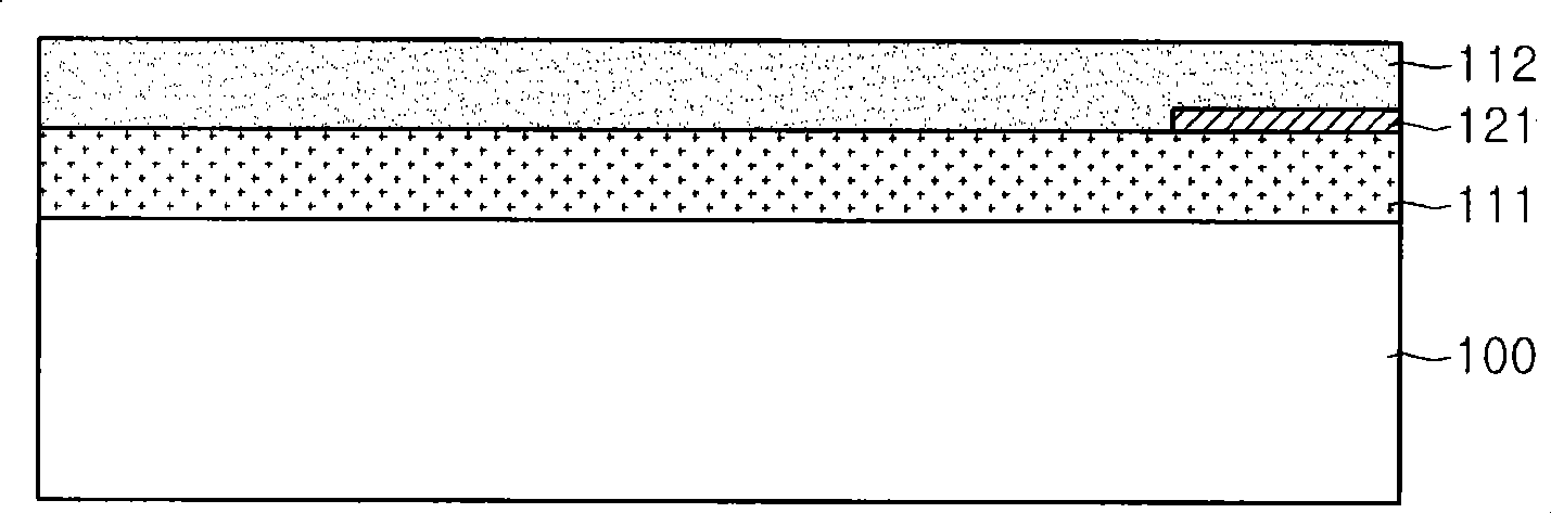
[0020] figure 1 is a plan view showing an inductor of a semiconductor device according to an embodiment of the present invention, and figure 2 is along figure 1 A cross-sectional view of the inductor obtained fro...


PUM


Abstract

A semiconductor device including an inductor and a fabricating method thereof are provided. The semiconductor device can include a connection wiring provided on a semiconductor substrate; a metal wiring provided on an insulating layer in a spiral shape and electrically connected to the connection wiring; and holes provided in the insulating layer and between the metal wiring and the silicon substrate.

Description

technical field [0001] The invention relates to a semiconductor device and a manufacturing method thereof. Background technique [0002] As technologies in the field of radio mobile communications have become more and more important, the demand for high-frequency resources and devices and circuits operating at high frequencies has also increased. Such devices typically include radio frequency (RF) components and integrated circuits (ICs). [0003] Furthermore, as technologies in the field of semiconductor processing have been developed, the high frequency characteristics of complementary metal oxide semiconductors (CMOS) have been greatly improved. Since CMOS is based on silicon, low-cost chips can be manufactured using well-developed process technologies, and it is also possible to integrate even mid-band and digital parts of the system using a system-on-chip (SOC) approach. Therefore, CMOS SOC is generally considered to be the best technology for manufacturing a single c...

Claims


Application Information

Patent Timeline
Patent Type & Authority Applications(China)
IPC IPC(8): H01L27/02H01L23/522H01L21/822H01L21/768
CPCH01L2924/0002H01L23/5227H01L2924/00H01F17/00H01F27/00
Inventor 金南柱
Owner DONGBU HITEK CO LTD
Why Eureka
Try Eureka