Preparation of ZnO back gate nano line field effect tube

A field effect transistor and nanowire technology, which is applied in semiconductor/solid-state device manufacturing, electrical components, circuits, etc., can solve problems such as inability to guide the device process and inability to optimize device structure, and achieve low cost, cost saving, and simple process. easy effect

Inactive Publication Date: 2009-03-11
SEMICON MFG INT (SHANGHAI) CORP +1
View PDF0 Cites 16 Cited by
  • Summary
  • Abstract
  • Description
  • Claims
  • Application Information

AI Technical Summary

Problems solved by technology

Moreover, the transport mechanism of nanowires has not been well simulated, and the d...

Method used


Image

  • Preparation of ZnO back gate nano line field effect tube
  • Preparation of ZnO back gate nano line field effect tube
  • Preparation of ZnO back gate nano line field effect tube

Examples


Embodiment Construction

[0027] The present invention will be described in further detail below in combination with specific embodiments and with reference to the accompanying drawings.

[0028] The invention provides a method for preparing a ZnO back-gate nanowire field effect transistor, the steps of which are as follows:

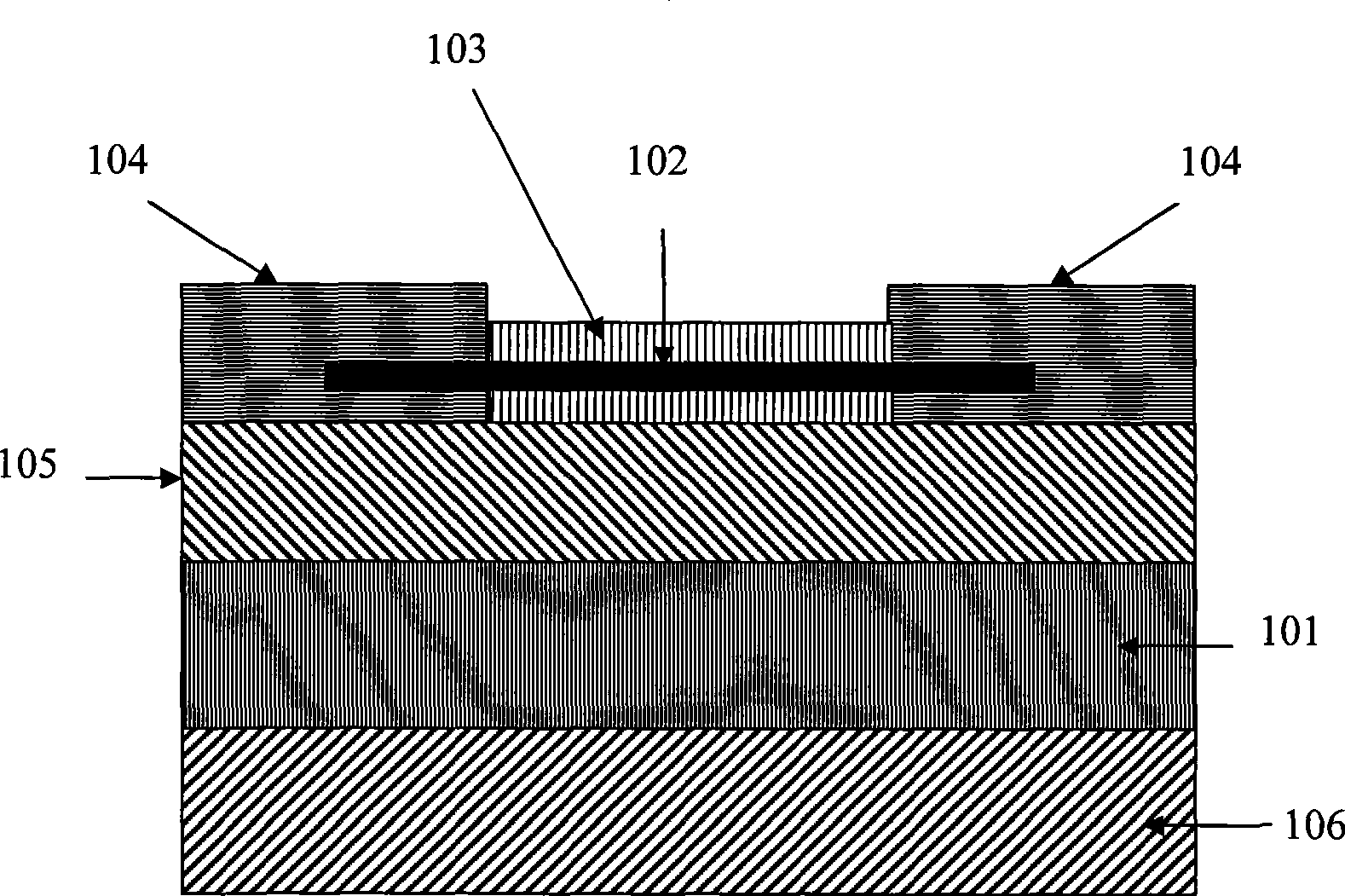
[0029] (1) at P ++ SiO grown on Si substrate 101 2 Dielectric layer 105, glue coating, pre-baking, RIE primer, and photolithography of the substrate by using a cross or groove plate;

[0030] The SiO 2 The thickness of the dielectric layer 105 is The glue coating is positive glue 5214, the rotation speed is 3500 rpm when the glue is uniform, and the thickness of the glue is 1.6 μm; the pre-baking is baking at 100 ° C for 60 seconds;

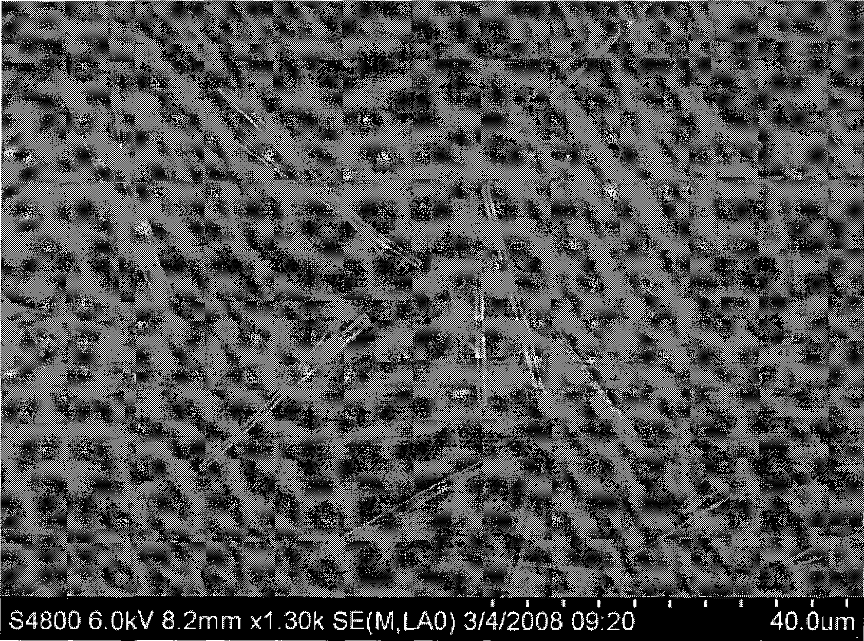
[0031] (2) Put the original growth ZnO nanowires 102 and the substrate in ethanol and undergo ultrasonic degradation. After the degradation, most of the ZnO nanowires 102 are detached from the original glass substrate and dispersed in the ethan...


PUM


Abstract

The invention relates to the technical field of a compound semiconductor device, in particular to a method for preparing a back gate ZnO nano wire field effect pipe. The method adopts a ZnO nano wire as a channel of a field effect transistor, the deposition and the position from the nano wire to a device substrate are realized by adopting a groove method and a cross method, the ohm contact is formed by adopting Ti/Au and a ZnO channel, Al2O3 gate oxygen is formed by a traditional Liff-off method in a spattering mode, and a P<++> type Si substrate is used as a back gate of the field effect pipe. The invention has the advantages of obvious effect, simple technology, easy operation, economy, applicability and high reliability, and is easy to adopt and popularize in the preparation of microwave and millimeter wave compound semiconductor devices and sensors.

Description

technical field [0001] The invention relates to the technical field of compound semiconductor devices, in particular to a preparation method of a ZnO back gate nanowire field effect transistor. Background technique [0002] Among various one-dimensional nanowire devices composed of ZnO nanowires, ZnO nanowire field-effect transistors have received extensive international attention in recent years due to their unique properties. ZnO nanowire field effect transistor (ZnO NW FET) is a field effect transistor realized by using ZnO nanowire as a channel. It is characterized in that it adopts a new MOSFET structure, and ZnO nanowire forms metal-oxide- semiconductor structure. Field effect transistors with this structure have potential wide applications in piezoelectric effect, optical effect, electromagnetic, chemical sensing and so on. Among them, due to the high surface area / volume ratio of ZnO nanowires, the successfully fabricated ZnO nanowire field effect transistors can al...

Claims


Application Information

Patent Timeline
IPC IPC(8): H01L21/336
Inventor 付晓君张海英徐静波黎明
Owner SEMICON MFG INT (SHANGHAI) CORP
Why Eureka
Try Eureka