Check patentability & draft patents in minutes with Patsnap Eureka AI!

Micro lead frame semiconductor packaging method

A lead frame and packaging method technology, which is applied in the field of new packaging manufacturing, can solve the problems of poor fragmentation of IC components, reduced reliability and penetration of micro-lead frame IC components, and achieves control of poor fragmentation and improvement of reliability. bad effect

Inactive Publication Date: 2009-03-11
PHOENIX SEMICON TELECOMM SUZHOU
View PDF0 Cites 9 Cited by
  • Summary
  • Abstract
  • Description
  • Claims
  • Application Information

AI Technical Summary

Problems solved by technology

When using the punch of the pressure equipment to separate from the lead frame into several individual IC components, the M.L.F type IC components have incompletely cut pins and connecting ribs, as well as pins and pins. The epoxy molding compound between the pins and the connecting ribs, and it will have a great impact on the IC components when cutting, and the IC may be between the pins and the pins and the connecting ribs. Cracks occur on the epoxy molding compound on the surface of the components, and in severe cases, the brokenness of the IC components is poor. These defects can easily cause external moisture to penetrate into the IC components, thereby reducing the reliability of the micro-lead frame IC components.

Method used


Image

  • Micro lead frame semiconductor packaging method
  • Micro lead frame semiconductor packaging method
  • Micro lead frame semiconductor packaging method

Examples


Embodiment Construction

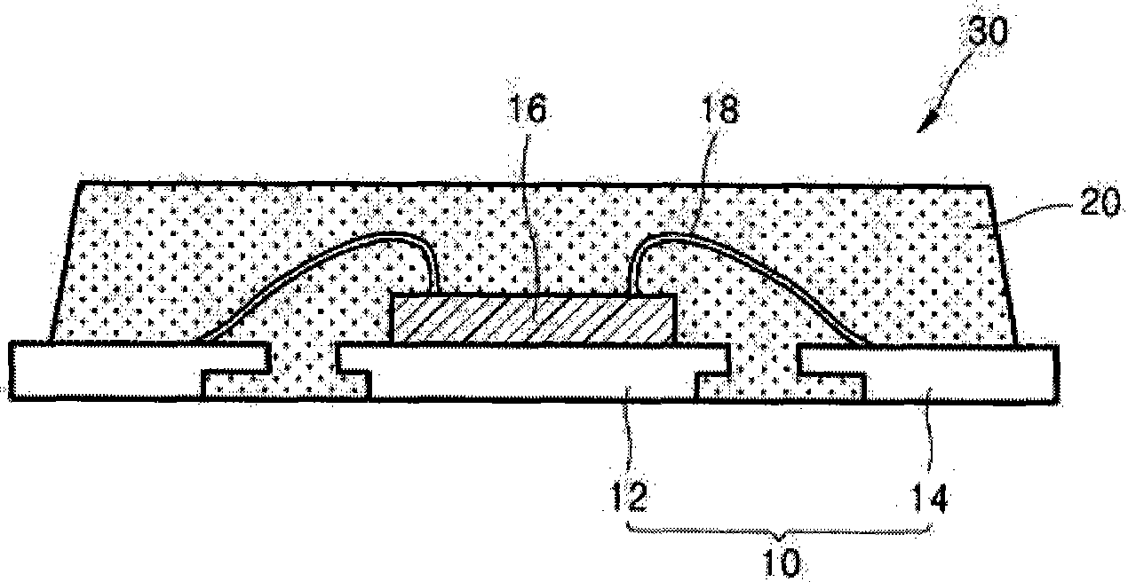
[0018] figure 1 It is a cross-sectional view of an M.L.F type IC component package of the prior art, and the M.L.F type semiconductor package 30 of the prior art is shown in the figure. The lead frame type lead frame 10 is composed of a chip pasted on the substrate and a lead 18 connecting the chip 16 and the pin 14 .

[0019] figure 2 It is a plan view of M.L.F packaged IC components in the prior art, the exposed portion 24 of the pin 14 of the lead frame 10, the exposed portion 22 of the connecting rib of the lead frame 10, and the exposed portion between the exposed pin and the pin. Epoxy molding compound 26.

[0020] image 3 It is a cross-sectional view of an M.L.F type packaged IC component of an embodiment of the present invention. The M.L.F type IC component package 30 of an embodiment of the present invention is shown in the figure. The micro-lead frame type lead frame 110 composed of pins 112 is composed of a chip pasted on the substrate and a lead 130 connectin...


PUM


Abstract

The invention relates to a method for encapsulating a micro leading wire frame type semiconductor, which comprises the following steps: (a) a micro leading wire frame type encapsulating leading wire frame is well prepared, next, a plurality of single IC chips are bonded on a base piece of the leading wire frame; (b) the chips and the leading wire frame are electrically connected by a golden wire through a leading wire bonding technology; (c) the semiconductor is formed, the upper part of the leading wire frame, the chips and the leading wire are encapsulated by using an epoxy encapsulating material, and the upper part of the leading wire which is arranged on the leading wire frame is not exposed outwards; (d) finally, the formed micro leading wire frame is divided into a plurality of single IC elements, and a pin and a connecting rib of each divided single IC element are covered by the epoxy encapsulating material. The method for encapsulating aims to separate the pin and the connecting rib which are not exposed and the M.L.F type semiconductor encapsulating IC elements of the epoxy encapsulating material between the pin and the connecting rib by a punching head of a pressure device and can furthest reduce the generated punching force in a punching process so as to increase the reliability of the M.L.F type semiconductor encapsulating elements.

Description

technical field [0001] The invention belongs to the technical field of semiconductor encapsulation technology, and relates to a novel encapsulation manufacturing method capable of effectively controlling the occurrence of epoxy molding compound cracks and poor breakage failures of the epoxy molding compound during the separation process using a punch of a pressure device. Background technique [0002] The volume of electronic products is gradually miniaturized, and the volume of semiconductor package IC (integrated circuit) components used in electronic products is also gradually miniaturized. M.L.F (miniature lead frame) type semiconductor package components are one of them. There are two types of M.L.F packaging methods, one is separated by cutting with a blade, and the other is separated by a punch of a pressure device. When using the punch of the pressure equipment to separate from the lead frame into several individual IC components, the M.L.F type IC components have in...

Claims


Application Information

Patent Timeline
IPC IPC(8): H01L21/50H01L21/56H01L21/60
CPCH01L2224/45144H01L2924/01079H01L2224/48091H01L2224/48465H01L2224/48247
Inventor 陶少卿
Owner PHOENIX SEMICON TELECOMM SUZHOU
Features
  • R&D
  • Intellectual Property
  • Life Sciences
  • Materials
  • Tech Scout
  • Unparalleled Data Quality
  • Higher Quality Content
  • 60% Fewer Hallucinations
Learn More