Forming method of resin lens in LED module

A technology of LED components and resin lenses, which is applied in semiconductor devices of light-emitting components, optical components, components of lighting devices, etc., can solve the problems of time-consuming curing process, lack of light transmission, and unfavorable mass production of LED components. Achieve the effects of shortening the curing process, saving equipment costs, and facilitating mass production

Inactive Publication Date: 2009-03-18
ISOTECH PRODS
View PDF2 Cites 27 Cited by
  • Summary
  • Abstract
  • Description
  • Claims
  • Application Information

AI Technical Summary

Problems solved by technology

[0004] However, in the packaging method of the above-mentioned existing LED components, the corresponding molding molds for molding the cover lens are generally made of metal materials, which do not have light transmission, so that the molds injected into the molding cavity The liquid light-transmitting resin only leaves a limited area exposed to the outside at the mouth of the molding cavity; but since the combination of the LED crystal grain and the base described in the packaging method is arranged at the opening of the molding cavity, the described The limited exposure area is partially covered, so that the exposure area between the liquid translucent resin injected into the molding cavity and the outside world is relatively smaller, so it is not conducive to or even difficult to use electron beams (EB, electron- beam) or ultraviolet (UV, ultraviolet ray) to cure (cure) the liquid translucent resin. Therefore, the current packaging method of LED components is generally to combine the molding mold with the liquid translucent resin injected into it. The resin is put into the oven at the same time for heating and baking. For example, it is generally baked at a temperature of about 120 degrees Celsius for 1 hour or more before the liquid translucent resin can be cured and formed, so that the entire curing process is quite time-consuming, which is not conducive to Mass production of LED components

Method used


Image

  • Forming method of resin lens in LED module
  • Forming method of resin lens in LED module
  • Forming method of resin lens in LED module

Examples


Embodiment Construction

[0023] In order to make the present invention more definite and detailed, the preferred embodiments are listed hereby together with the following diagrams, and the structure and technical characteristics of the present invention are described in detail as follows:

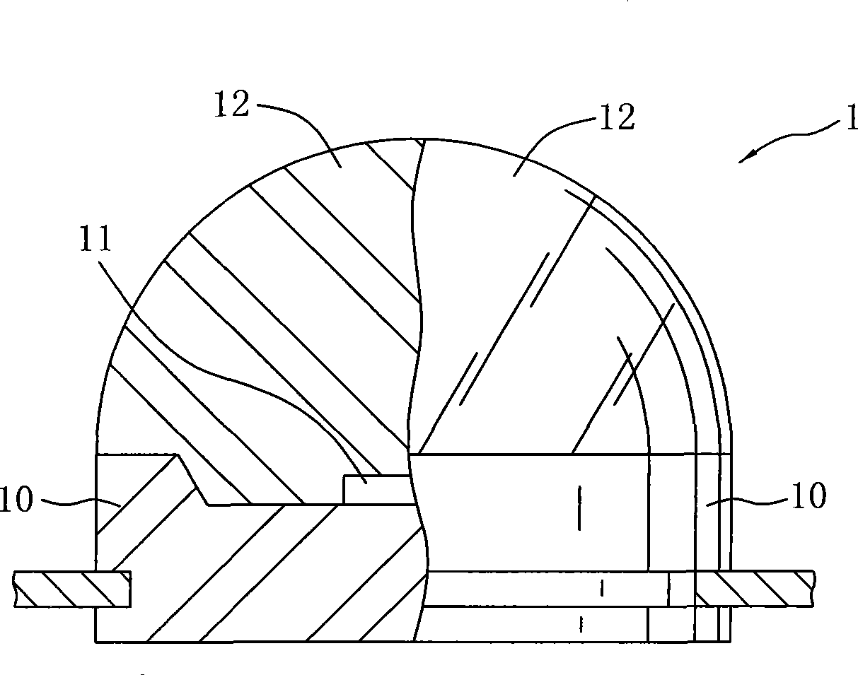
[0024] refer to figure 1 As shown, it is a schematic side view of an existing general LED assembly. The LED assembly 1 can be designed to have various packaging structures, and generally includes: a base 10 for carrying the LED die 11 and electrically connecting with the LED die 11, so that the LED die can be connected to an external power source to emit light ; one or several LED crystal grains 11, which can emit light after being connected to an external power supply; and one or more layers of cover lenses (cover lens) 12 formed by light-transmitting resin materials, used to cover the base 10 On the outside of the LED crystal grain 11, the base 10 and the LED crystal grain 11 are packaged into an LED component 1...


PUM


Abstract

The invention provides a method for forming resin lenses in an LED component, which comprises the following steps: manufacturing a mould corresponding to the lens by a material with light transmittance, which contains plastic materials, such as PP, PET, PC, PE, or glass and the like; selecting liquid light-transmittance resin material for forming the lens, such as polyurethane, epoxide resin, silica gel, polyacrylic resin or co-polymer thereof and the like; quickly solidifying the liquid light-transmittance resin under irradiation of electron beam, or adding light trigger in the materials to solidify the liquid light-transmittance resin under irradiation of ultraviolet ray. By being combined with the LED component, the resin can be injected in the mould corresponding to the lens, and the resin material inside the mould is irradiated by the electron beam or the ultraviolet ray from the outside of the light-transmittance mould, so that the resin material can be quickly solidified and formed into the lens. Therefore, the solidifying process of the lens can be accelerated, and the solidified forming time of the resin can be effectively shortened.

Description

technical field [0001] The invention relates to a molding method of a resin lens body in an LED component, especially a resin material with light transmission, such as PP (polypropylene), PET (polyethylene terephthalate), PC ( polycarbonate), PE (polyethylene) or glass materials etc. to make molds to prepare the method of the resin lens body. Background technique [0002] The existing light-emitting diode assembly (LED assembly) or light-emitting diode optical module can be designed with various packaging structures, different light-emitting patterns or different methods according to the use or structural needs, such as China Taiwan M297481, M294096, 1246787、1246779、M283326、M283312、M281294、M268724、M297046、M294808、M291602、M291085、M289908、M289521、M288974、M288005、M287503、200629598、200628727、200629598、200635085、200414558等新型或发明专利案,以及美国公开号 Pub.No.US2006 / 0105485A1, etc.; a general light-emitting diode assembly (LED assembly) mainly includes: a base for carrying LED crystal grains a...

Claims


Application Information

Patent Timeline
Patent Type & Authority Applications(China)
IPC IPC(8): B29C35/08B29C33/38F21V5/04B29K75/00B29K63/00B29K83/00B29K33/04B29L11/00F21Y101/02F21Y115/10
Inventor 李煌宝
Owner ISOTECH PRODS
Why Eureka
Try Eureka