Etching composite
A composition and etching technology, which is applied in the direction of electrical components, semiconductor/solid-state device manufacturing, circuits, etc., can solve problems such as difficult taper angles, and achieve the effect of reducing process steps
- Summary
- Abstract
- Description
- Claims
- Application Information
AI Technical Summary
Problems solved by technology
Method used
Image

Examples
Embodiment 1
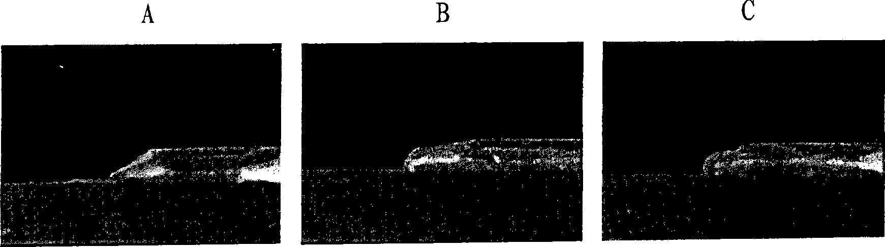
[0040] The etching composition was prepared with 2.5% by weight of triammonium phosphate trihydrate, 1.5% by weight of acetic acid monoethanolamine salt, 1.5% by weight of hydrogen peroxide, and the balance of water. The prepared etching composition (pH 9.05) was used. 3-layer laminated metal layer patterned by photoresist (Cu: 2000 , Each Mo alloy: 500 , A total of 3000 ) Substrate, the three-layer laminated metal layer is made of Cu and Mo alloy (I) (with 5 wt% Nb added Mo) or Cu and Mo alloy (II) (with 10 wt% Nb added Mo) The formed Mo alloy / Cu / Mo alloy laminated metal layer. The etching treatment is performed at a treatment temperature of 23°C, and the treatment time is the time until the metal layer is dissolved (Just. Etch. Time.). Through the etching process under the above conditions, the scanning electron micrographs of the tapered cross-section of the wiring obtained are as follows: figure 1 A(Mo5Nb / Cu / Mo5Nb) (using Mo alloy (I)), figure 1 B(Mo10Nb / Cu / Mo10Nb) (using...
Embodiment 2
[0043] The etching composition was prepared with 2.5% by weight of ammonium phosphate trihydrate, 3.75% by weight of acetic acid monoethanolamine salt, 1.5% by weight of hydrogen peroxide and the balance of water, and the prepared etching composition (pH 8.95) was used. Photoresist patterned three-layer laminated metal layer of Mo alloy / Cu / Mo alloy formed of Cu and Mo alloy (Mo with 10% by weight of Nb added) (Cu: Each Mo alloy: total ) Of the substrate. The etching treatment was performed at a treatment temperature of 23°C, and the treatment time was the time until the metal layer was dissolved (Just. Etch. Time.). Through the etching process under the above conditions, the obtained scanning electron micrograph of the tapered cross-section of the wiring is as follows: figure 1 C (Mo10Nb / Cu / Mo10Nb) shown.
[0044] by figure 1 It can be seen from C that the three-layer laminated metal layer of Cu and Mo alloy can be etched at the same time, and there is no side etching, and a ...
Embodiment 3
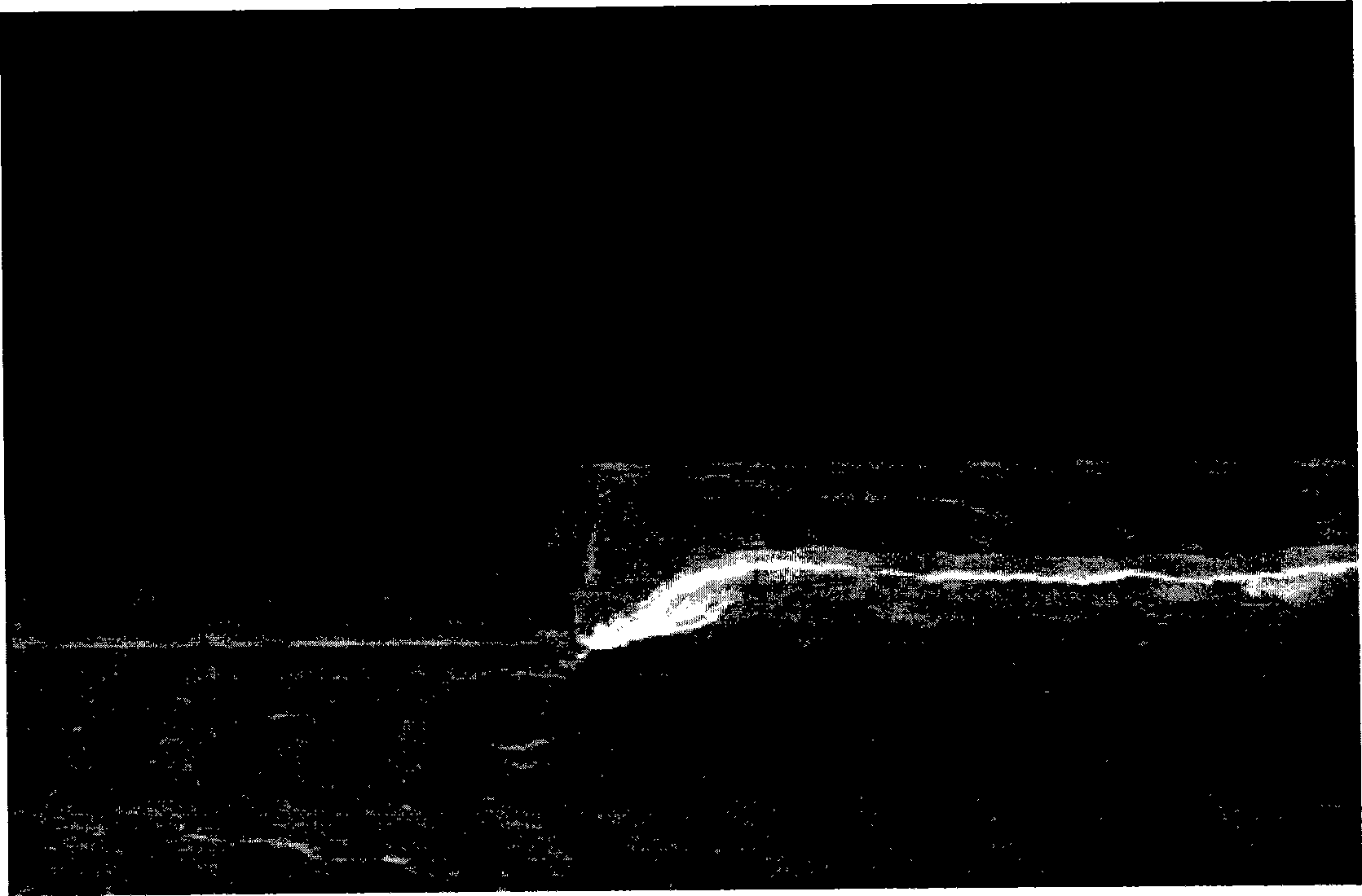
[0047] The etching composition was prepared with 2.5% by weight of triammonium phosphate trihydrate, 1.0% by weight of acetic acid monoethanolamine salt, 0.75% by weight of hydrogen peroxide, and the balance of water. The prepared etching composition (pH 9.07) was used. A two-layer laminated metal layer of Mo / Cu composed of Cu and Mo patterned with a photoresist (Cu: Mo: total ) Of the substrate. The etching treatment is performed at a treatment temperature of 25°C, and the treatment time is the time until the metal layer is dissolved (Just. Etch. Time.). Through the etching treatment under the above-mentioned conditions, the scanning electron micrograph of the tapered cross-section of the wiring obtained is shown figure 2 .
[0048] by figure 2 It can be seen that the two-layer laminated metal layer of Cu and Mo can be etched at the same time, and there is no side etching, and a good cross-sectional taper is obtained.
PUM
 Abstract
Description
Claims
Application Information
 - Generate Ideas
- Intellectual Property
- Life Sciences
- Materials
- Tech Scout
- Unparalleled Data Quality
- Higher Quality Content
- 60% Fewer Hallucinations
Browse by: Latest US Patents, China's latest patents, Technical Efficacy Thesaurus, Application Domain, Technology Topic, Popular Technical Reports.
© 2025 PatSnap. All rights reserved.Legal|Privacy policy|Modern Slavery Act Transparency Statement|Sitemap|About US| Contact US: help@patsnap.com