Output buffer circuit

A technology for output buffering and buffering circuits, applied in the direction of logic circuit connection/interface layout, etc., can solve the problems of high circuit noise and slow circuit conversion speed, and achieve the effect of small output resistance, fast conversion speed, and reduction of short-circuit current.

Inactive Publication Date: 2010-08-11
HUAZHONG UNIV OF SCI & TECH
View PDF0 Cites 1 Cited by
  • Summary
  • Abstract
  • Description
  • Claims
  • Application Information

AI Technical Summary

Problems solved by technology

In the design of the output buffer circuit, the main concerns of the predecessors include: drive capability, low power consumption, slew rate and other performance, less involving noise resistance and load adaptation
Through theoretical calculation and simulation analysis, it can be seen that under certain conditions of capacitance C and inductance L, the smaller the output resistance R of the RLC circuit shown in Figure 1(b), the faster the switching speed of the circuit, but at this time the noise of the circuit is also higher. In addition, the larger the output resistance, the smaller the noise of the circuit, but the switching speed of the circuit becomes slower

Method used


Image

  • Output buffer circuit
  • Output buffer circuit
  • Output buffer circuit

Examples


Embodiment Construction

[0013] The present invention will be described in further detail below in conjunction with accompanying drawing and example.

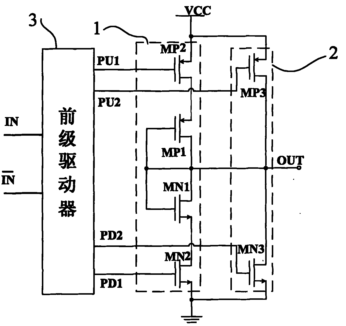
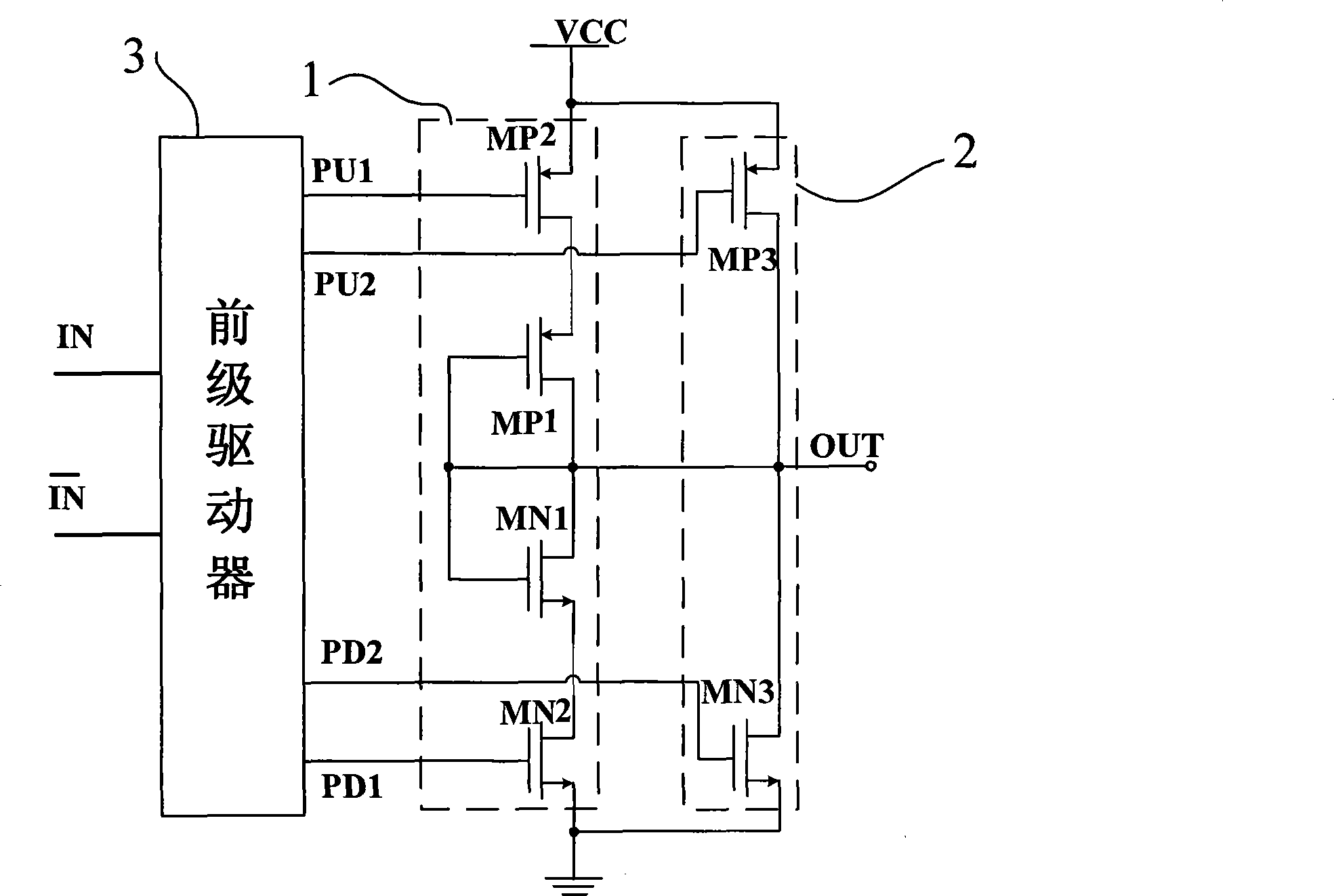
[0014] As shown in FIG. 2 , the high-speed output buffer circuit provided by the present invention includes a pre-stage driver 3 , a first charging and discharging circuit 1 and a second charging and discharging circuit 2 . The input of the pre-stage driver 3 is the input signals IN and IN of the high-speed output buffer circuit, where IN is the inverse signal of IN, and the output of the pre-stage driver 3 is the output control signals PU1, PU2, PD1 and PD2. The function of the pre-stage driver is to provide control signals with a certain timing relationship for the two charging and discharging circuits, and to increase the driving capabilities of the two charging and discharging circuits step by step.

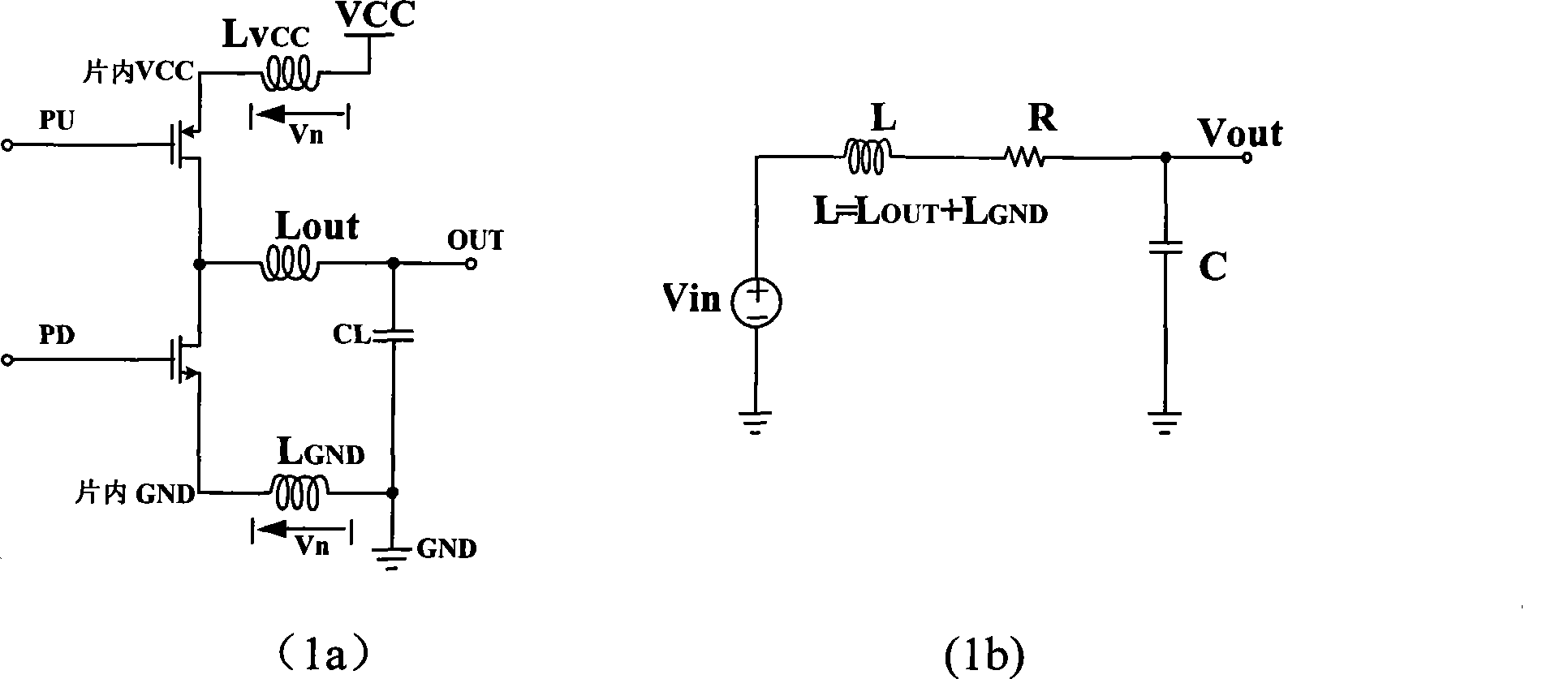
[0015] The first charging and discharging circuit 1 is composed of first and second PMOS transistors MP2 and MP1 and first and second NMOS transistor...


PUM


Abstract

The invention discloses an output buffer circuit which has noise resistant and load adaptive capacity. The buffer circuit comprises a pre-driver, a first charge and discharge circuit and a second charge and discharge circuit. The pre-driver provides the first charge and discharge circuit and the second charge and discharge circuit with a drive signal so as to enable the first charge and dischargecircuit and the second charge and discharge circuit to be electrified at different times; the PMOS tube which is connected in a diode manner and the NMOS tube which is connected with a diode in the first discharge circuit cut off automatically when the charge and discharge is almost over, thereby enhancing a resistance which can be seen from an output end and ensuring the circuit has excellent noise resistant property. Additionally, the structure of the invention can lead the electrification time of two discharge circuits to take up the proportion size of the overall switching process, that is, the driving capacity provided by the circuits changes along with the change of a load, so that load adaptive capacity is possessed. Therefore, the invention has the advantages of low consumption, noise resistance, and load adaptive property.

Description

technical field [0001] The invention belongs to the field of microelectronic integrated circuits, and in particular relates to a low-noise, load-adaptive high-speed output buffer circuit, which is especially suitable for occasions where the output load of a chip changes and the noise performance is high. Background technique [0002] The output buffer circuit provides connections between the internal circuit of the chip and the external circuit. It is used in occasions where the core voltage of the chip is different from the external voltage of the chip. The high-speed output buffer circuit can provide voltage conversion, increase the driving capability of the circuit, and reduce output ringing. , these functions make the output buffer circuit widely used in the output of digital chips and the interface of digital and analog circuits. In the design of the output buffer circuit, the main concerns of the predecessors include: driving capability, low power consumption, slew rat...

Claims


Application Information

Patent Timeline
Patent Type & Authority Patents(China)
IPC IPC(8): H03K19/0175
Inventor 邹雪城刘政林林映嫣王双洋雷鑑铭高专李伟杨蕾
Owner HUAZHONG UNIV OF SCI & TECH
Why Eureka
Try Eureka