

Manufacturing and repairing method for conductive circuit of three dimensional mold interconnecting device
A technology for molding interconnection and conductive lines, applied in the directions of printed circuit manufacturing, printed circuit, conductive pattern formation, etc., can solve the problems of high price, low wear resistance, high 3D-MID cost, and reduce material cost , Environmentally friendly and efficient
Active Publication Date: 2010-12-01
WUHAN XINRUIDA LASER ENG
View PDF1 Cites 0 Cited by
- Summary
- Abstract
- Description
- Claims
- Application Information
AI Technical Summary
Problems solved by technology
Some large integrated parts can be produced through injection compounding, such as door panels and center pillars of automobiles, but due to the processing method, the three-dimensional structure design is limited and cannot be used to produce products with complex structures
With the development of plastic electronic products in the direction of miniaturization, light weight, high density, low cost, small batch, diversification, and environmental protection, there are some deficiencies in the above 3D-MID manufacturing technology: first, it is moldable with plating The base material of structural parts is expensive. For example, in order to obtain platable plastics, the secondary two-component injection method often adds precious metals such as palladium (Pd) and gold (Au) to the plastics to obtain the so-called catalytically activated platable plastics (LCP- Pd or LCP-Au), in addition to the high price of adding elements Pd and Au, the catalyst used in this kind of catalytic activation can be plated plastic is very expensive, although the secondary two-component injection method is particularly suitable for the production of microstructures with fine structure components, but the final 3D-MID product cost is higher
However, the laser direct writing electronic paste method only relies on laser heat to remelt and solidify the binder phase in the electronic paste, and bonds various components together to form conductive lines. In this process, the performance of the substrate itself is basically No change, the functional wire is bonded to the substrate only by the bonding effect of the bonding phase, so the adhesion between the conductive layer and the substrate is not strong, and the wear resistance is not high
Method used
View moreImage
Smart ImageViewing Examples

Examples
Embodiment 1
Embodiment 2
Embodiment 3
Login to View More PUM
 Abstract
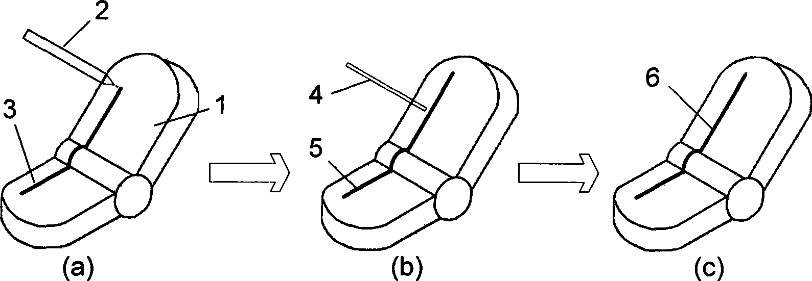
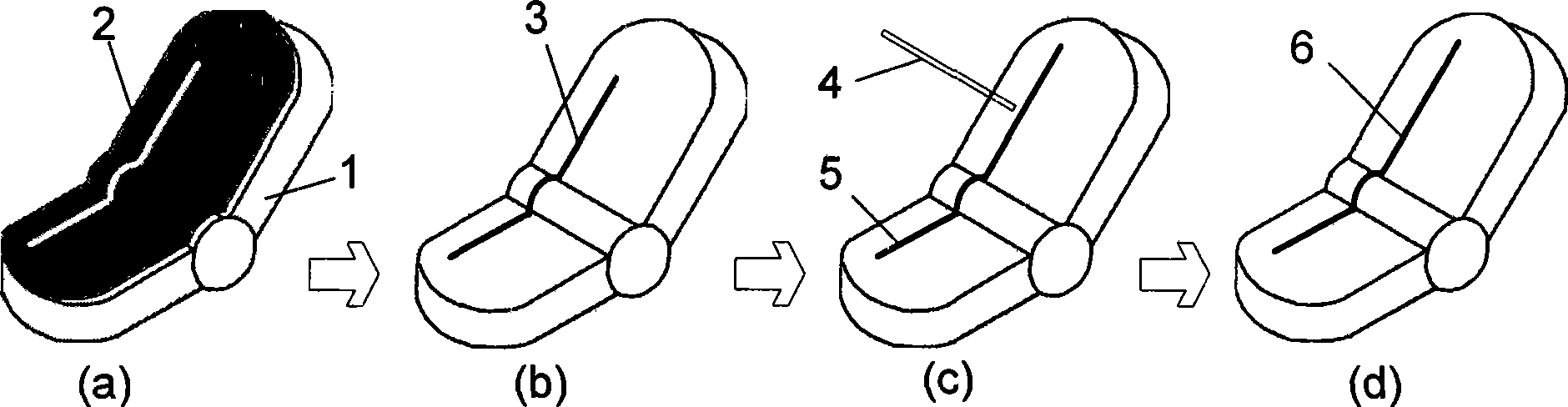
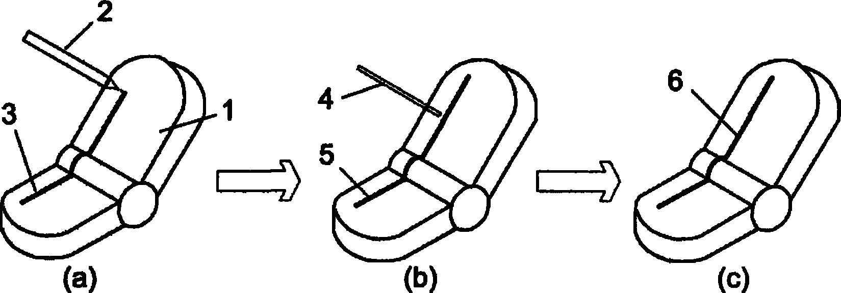
The invention discloses a method for manufacturing and repairing a three-dimensional molding interconnection device conductive line. The method comprises the following steps: (1) depositing a 0.1-50 micrometer thick prearranged sizing agent layer of a conductive sizing agent on the surface of a molding structural element according to the design configuration of a conductive line; (2) baking or airing the prearranged layer of the conductive sizing agent, and removing an organic solvent thereof; (3) utilizing a laser beam to irradiate the prearranged sizing agent layer so as to enable metal conductive particles in the sizing agent to be melted and mixed with a 5-500mum thin layer of the surface of a plastic matrix, and the metal conductive particles in the sizing agent to be embedded in thesurface of the matrix, thereby obtaining a conductive pattern; and (4) conducting chemical plating of 2-10mum copper on the surface of the conductive pattern, and then conducting chemical plating of 1-3mum anticorrosion metal. By the method, various complex conductive lines can be quickly and directly manufactured or repaired on the surface of three-dimensional molding structural member of various plastic matrix. No platability is required for base materials or no special requirement is needed for the molding technical. The invention has the advantages of simple process, environment-friendliness, low cost and high flexibility.
Description
A method for manufacturing and repairing conductive lines of three-dimensional molded interconnection devices technical field The invention belongs to the technical field of manufacturing and repairing conductive circuits and the technical field of laser micromachining, and relates to a method for manufacturing and repairing conductive circuits of three-dimensional molded interconnection devices. Specifically, laser micro cladding technology is used in the manufacture and repair of interconnection circuits on the surface of three-dimensional molded interconnection devices. Background technique Three-dimensional molded interconnect device (Three-dimensionalmouldedinterconnectdevice, 3D-MID) refers to the production of wires and graphics with electrical functions on the molded plastic shell, so as to integrate the electrical interconnection function and support of ordinary circuit boards. The functions of the components and the support and protection of the plastic shell are...
Claims
Login to View More Application Information
Patent Timeline
 Patent Type & AuthorityPatents(China)
IPC IPC(8): H05K3/10H05K3/20
Inventor曾晓雁曹宇李祥友刘建国
OwnerWUHAN XINRUIDA LASER ENG