Semiconductor light emitting element

A technology for light-emitting elements and semiconductors, which can be applied to semiconductor devices, electrical components, circuits, etc., and can solve problems such as hindering high brightness.

Inactive Publication Date: 2009-03-25
ROHM CO LTD
View PDF2 Cites 7 Cited by
  • Summary
  • Abstract
  • Description
  • Claims
  • Application Information

AI Technical Summary

Problems solved by technology

Therefore, in the semiconductor light-emitting element X, the proportion of the light that can be properly emitted in the light emitted by the active layer 93 is very small, which hinders the improvement of brightness.

Method used


Image

  • Semiconductor light emitting element
  • Semiconductor light emitting element
  • Semiconductor light emitting element

Examples


Embodiment Construction

[0079] Hereinafter, preferred embodiments of the present invention will be specifically described with reference to the accompanying drawings.

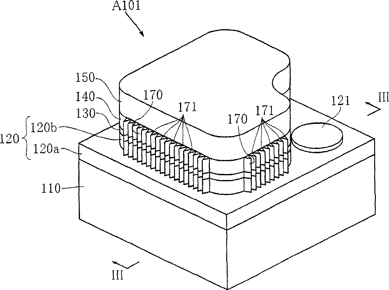
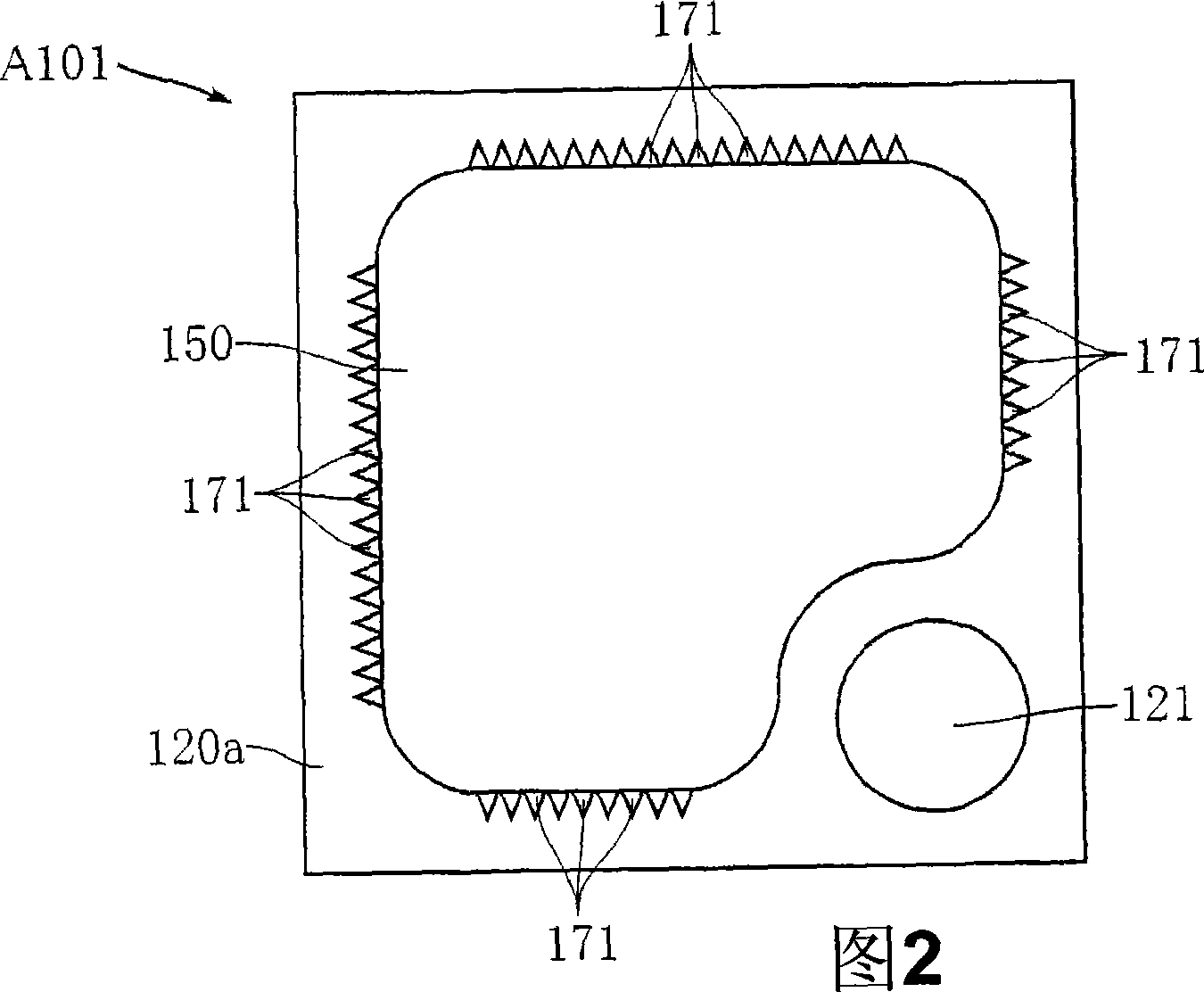
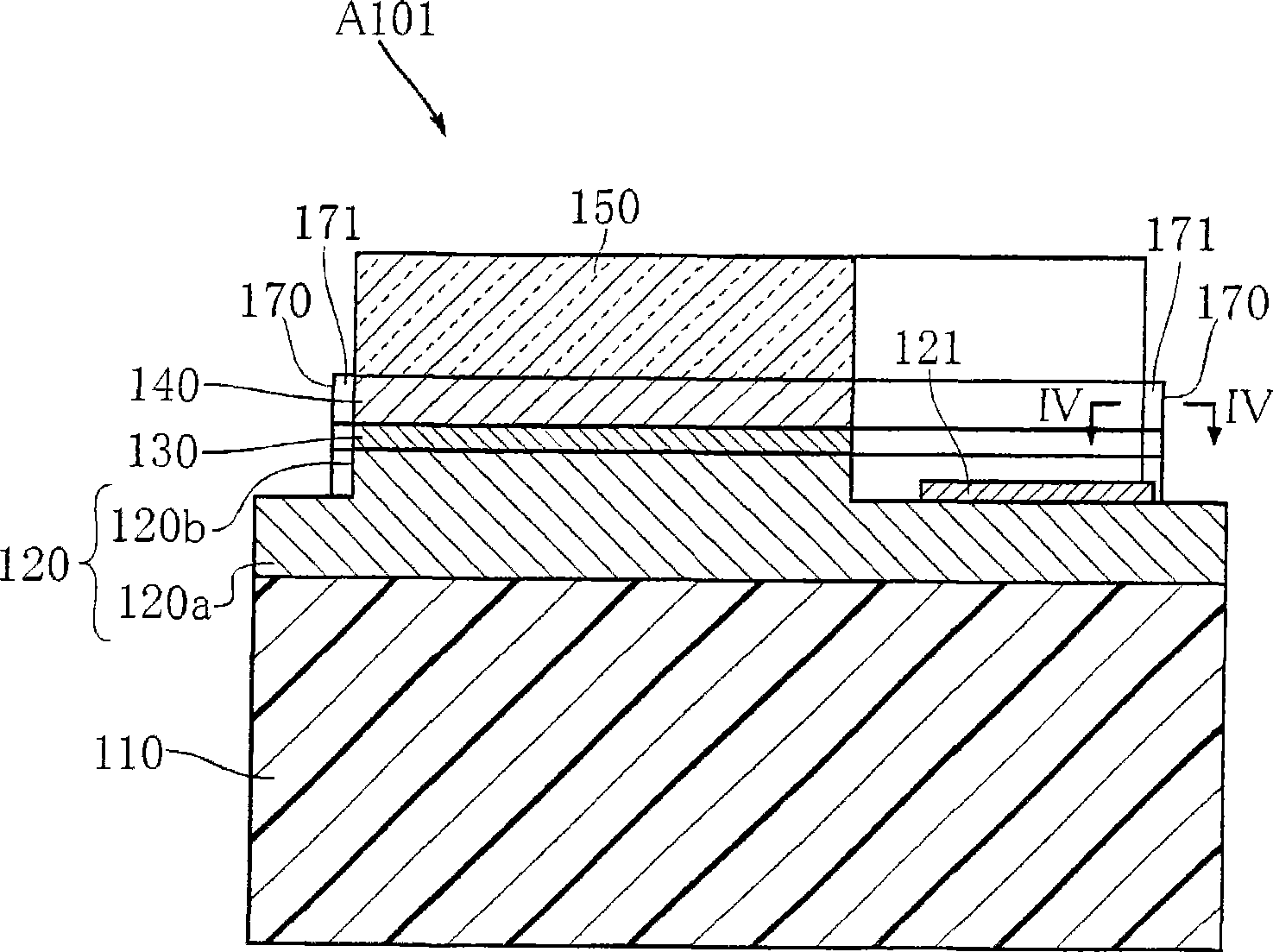
[0080] Figure 1 to Figure 3 This is the first embodiment of the semiconductor light-emitting element of the present invention. The semiconductor light-emitting element A101 of the present embodiment includes a substrate 110 , an n-GaN layer 120 , an active layer 130 , a p-GaN layer 140 , and a ZnO electrode 150 . The semiconductor light-emitting element A101 is constituted as a semiconductor light-emitting element particularly suitable for emitting blue light or green light.

[0081] The substrate 110 , eg, made of sapphire, is used to support the n-GaN layer 120 , the active layer 130 , the p-GaN layer 140 and the ZnO electrode 150 . In this embodiment, the thickness of the substrate 110 is about 80 μm. On the substrate 110 , for example, a buffer layer (not shown) made of AlN, GaN, AlGaN, or the like for alleviating lattice dist...


PUM


Abstract

In a semiconductor light emitting element, a p-type layer (220), an active layer (230) and an n-type layer (240) are laminated on a substrate in this order. The n-type layer (240) is formed with a rectangular n-side electrode (241) whose width in one direction is equal to that of the n-type layer (240). The thickness t of the n-type layer (240) satisfies Formula 1 below. The semiconductor light emitting element includes a side surface (270) extending in the lamination direction and formed with a plurality of projections (271). Supposing that the wavelength of the light from the active layer (230) is lambada, and the index of refraction of the n-type layer (240) or the p-type layer (220) is n, the average WA of widths at bottoms of the projections is set to satisfy WA >= lambada/n. In formula 1, L is width of the n-type layer in a direction different from the one direction, T is absolute temperature, W is width of the n-side electrode in a direction different from the one direction, J 0 is current density at the contact portion between the n-side electrode and the n-type layer, e is elementary charge, gamma is diode ideality factor, kappa is Boltzmann constant, rho is specific resistance of the n-type semiconductor layer.

Description

technical field [0001] The present invention relates to a semiconductor light-emitting element having a semiconductor layer. Background technique [0002] Heretofore, a semiconductor light-emitting element having a structure in which a plurality of semiconductor layers including GaN are stacked on a sapphire substrate has been proposed (eg, Patent Document 1). [0003] In addition, as one method of manufacturing a semiconductor light-emitting element, it is known to form a semiconductor layer on a sapphire substrate, bond a support substrate to a portion of the semiconductor layer on the opposite side of the sapphire substrate, and heat by a laser. A method of peeling off the above-mentioned sapphire substrate (for example, refer to Patent Document 2). Figure 20 An example of a semiconductor light-emitting element manufactured by this manufacturing method is shown. The semiconductor light-emitting element X shown in the figure is structured such that a p-GaN layer 92, an a...

Claims


Application Information

Patent Timeline
Patent Type & Authority Applications(China)
IPC IPC(8): H01L33/00H01L33/06H01L33/32
CPCH01L33/22
Inventor 酒井光彦冈崎忠宏中原健
Owner ROHM CO LTD
Why Eureka
Try Eureka