Gallium nitride based transistor structure with high electron mobility

A high electron mobility, gallium nitride-based technology, applied in the structural field of gallium nitride-based high electron mobility transistors, can solve the problem that the performance of the corresponding device with electron mobility is difficult to be further improved, and the uneven scattering effect of alloy composition , device performance deterioration, etc.

Inactive Publication Date: 2009-04-01
INST OF SEMICONDUCTORS - CHINESE ACAD OF SCI
View PDF0 Cites 24 Cited by
  • Summary
  • Abstract
  • Description
  • Claims
  • Application Information

AI Technical Summary

Problems solved by technology

In this traditional structure, a triangular potential well is formed at the heterojunction of AlGaN and GaN. The potential barrier on one side of the gallium buffer layer is lower, and the electrons in the channel will cross the potential barrier on the side of the gallium nitride buffer layer in the triangular potential well, which will deteriorate the device performance; The aluminum composition is low, so the increase of the conduction band discontinuity parameter on the AlGaN side at the interface between AlGaN and GaN heterojunction is limited, and the inhomogeneity of the alloy composition in AlGaN has a negative impact on The scattering effect of the traditional structure makes it difficult to further improve the electron mobility and the performance of the corresponding device.

Method used


Image

  • Gallium nitride based transistor structure with high electron mobility
  • Gallium nitride based transistor structure with high electron mobility
  • Gallium nitride based transistor structure with high electron mobility

Examples


Embodiment Construction

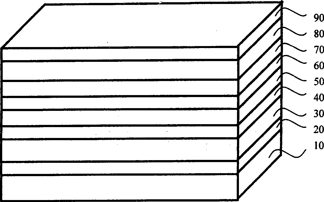
[0029] see figure 1 As shown, the present invention has invented a GaN-based high electron mobility transistor structure, which includes:

[0030] (1) substrate 10, the material of the substrate 10 is sapphire or silicon or silicon carbide or gallium nitride or aluminum nitride or ZnO;

[0031] (2) low temperature nucleation layer 20, this low temperature nucleation layer 20 is gallium nitride or aluminum nitride or AlGaN, is made on the substrate 10, and the effect of low temperature nucleation layer 20 is to provide effective for the growth of epitaxial layer Nucleation center, and because a large number of dislocations generated release most of the stress of the epitaxial layer, effectively reducing the dislocation density of the epitaxial layer, improving the crystal quality of the material and the performance of the device;

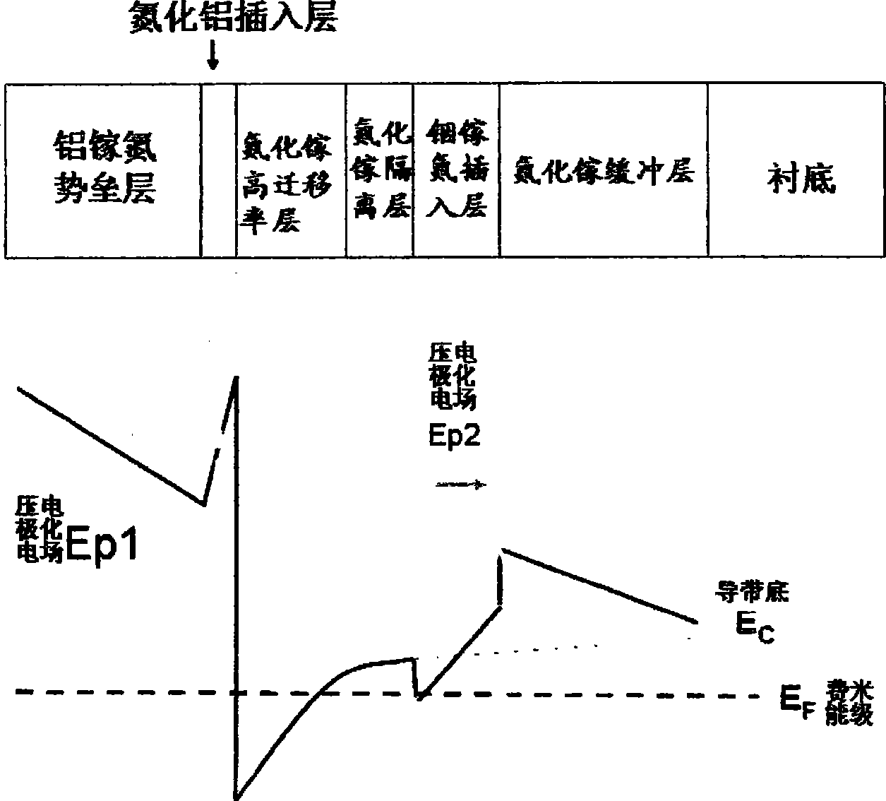
[0032] (3) gallium nitride high resistance layer 30, the gallium nitride high resistance layer 30 is fabricated on the low-temperature nucleation l...


PUM

PropertyMeasurementUnit
thicknessaaaaaaaaaa
thicknessaaaaaaaaaa
thicknessaaaaaaaaaa

Abstract

A gallium nitride-based high electron mobility transistor structure comprises: a substrate; a low temperature nucleating layer is produced on the substrate; a gallium nitride-based high resistivity layer is produced on the low temperature nucleation layer; an indium gallium nitride insertion layer is produced on the gallium nitride-based high resistivity layer; a low temperature gallium nitride isolation layer is produced on the indium gallium nitride insertion layer; a high mobility gallium nitride layer is produced on the low temperature gallium nitride isolation layer; an aluminum nitride insertion layer is produced on the high mobility gallium nitride layer; an aluminium gallium nitride barrier layer is produced on the aluminum nitride insertion layer; a gallium nitride cap layer is produced on the aluminium gallium nitride barrier layer, and the gallium nitride cap layer effectively inhibit the current collapse effect.

Description

technical field [0001] The invention belongs to the field of semiconductor science and technology, in particular to a structure of a gallium nitride-based high electron mobility transistor. Background technique [0002] GaN-based high electron mobility transistors have the characteristics of high temperature, high frequency, high power and radiation resistance, can work in harsh environments, and have broad application prospects in radar, satellite communication, wireless communication and other fields. [0003] The principle of gallium nitride-based high electron mobility transistors is: due to the conduction band discontinuity of the two materials gallium nitride and aluminum gallium nitride, and due to the spontaneous polarization and piezoelectric polarization effects of these two materials, in A triangular potential well is formed at their interface, thereby forming a two-dimensional electron gas in the triangular potential well. Since the two-dimensional electron gas a...

Claims


Application Information

Patent Timeline
Patent Type & Authority Applications(China)
IPC IPC(8): H01L29/778
Inventor 王晓亮唐健肖红领王翠梅冉学军胡国新李晋敏
Owner INST OF SEMICONDUCTORS - CHINESE ACAD OF SCI
Why Eureka
Try Eureka