
Organic thin-film transistor and method for controlling surface energy of polymer material layer

A technology of polymer materials and organic thin films, applied in semiconductor/solid-state device manufacturing, electrical solid-state devices, semiconductor devices, etc., can solve the problems that plastic substrates cannot withstand high temperatures and are not suitable for plastic substrates

Active Publication Date: 2009-04-01
IND TECH RES INST
View PDF0 Cites 4 Cited by
  • Summary
  • Abstract
  • Description
  • Claims
  • Application Information

AI Technical Summary

Problems solved by technology

[0005] However, the currently used cross-linking PVP macromolecule dielectric material, such as described in J.Appl.Phys.92, 5292 (2002) or Appl.Phys.Lett.87, 152105 (2005), requires a process temperature of It can be as high as 180℃~200℃, and the heating time needs to be more than 1 hour. However, the plastic substrate used in general flexible displays cannot withstand high temperature, so the traditionally used cross-linked PVP polymer dielectric material is not suitable for use as Plastic substrates used in large flat panel displays

Method used


Image

  • Organic thin-film transistor and method for controlling surface energy of polymer material layer
  • Organic thin-film transistor and method for controlling surface energy of polymer material layer
  • Organic thin-film transistor and method for controlling surface energy of polymer material layer

Examples


Embodiment 1~2

[0059] The composition of the dielectric layer material formula solution is: 10wt% PVP+5wt%PMF+3wt%PAG+82wt%PGMEA

[0060] Get polymer PVP (molecular weight Mw is 20000, produced by Aldrich company) 0.1g, crosslinking agent PMF (molecular weight Mw is 500, produced by Aldrich company) 0.05g and photoacid generator (PAG) (4-[(2-hydroxy deca Tetraalkyl) oxygen] phenyl) phenyliodonium-hexafluoroantimonate ((4-[(2-Hydroxytetradecyl)oxy]phenyl)phenyliodonium hexafluoroantimomnate) 0.03g (produced by Aldrich Company), use PGMEA (produced by Tedia Company) As a solvent, it is prepared into a formula solution containing 10wt% PVP, 5wt% PMF and 3wt% PAG.

[0061] Film preparation: after filtering the above formulation solution with a 0.2 μm filter, the solution was coated on a silicon wafer (wafer) by spin coating (rotation speed 1000 rpm, time 30 sec). After the coated film was irradiated with 365nm UV light for 1 minute, the film of Example 1 was baked at 100°C for 5 minutes, and th...

Embodiment 3~7

[0070] The composition of the dielectric layer material formula solution is: 11wt% PVP+4wt%PMF+2wt%PAG+83wt%PGMEA

[0071] Get the polymer PVP0.11g identical with embodiment 1, cross-linking agent PMF0.04g and photoacid generator (PAG) 0.03g, use PGMEA as solvent and be formulated into containing 11wt%PVP, 4wt%PMF and 2wt%PAG Formula solution. A thin film was prepared in the same manner as in Example 1, and irradiated with 254nm UV light for 10 minutes. The baking temperature / time and PGMEA test results are listed in Table 2.

[0072] Surface energy test: The surface energy of the films of Examples 3 to 7 was measured by contact angle measurement (using a FACE contact angle meter, Kyowa Kaimenkagaku Co.), using distilled water and diiodomethane CH 2 I 2 (di-iodomethane) is used as a detection liquid, and the surface energy is calculated by measuring the contact angle of distilled water and diiodomethane on the film surface.

[0073] The PGMEA test and the surface energy tes...

Embodiment 8~10

[0078] The materials used in Examples 8-10 are the same as those in Example 1, and the composition of its formulation solution is listed in Table 3 below. The formulation solution of Examples 8-10 is made into a film in the same film preparation mode as in Example 1. The baking temperature is 120° C., and the baking time is 30 minutes. Next, the films of Examples 8-10 were subjected to PGMEA test and surface energy test, and the results are listed in Table 3 below.


PUM


Abstract

The invention relates to an organic thin film transistor, wherein, a dielectric layer is composed of a composite, the composite comprises: (a) a polymer, the structure of the repeated unit is shown in formula (I), wherein, each X is H or C1-54 alkyl respectively and independently; each R is H, alkyl, acetoxyl group, tert-butyl, beta-methoxy ethoxy methyl ether, methoxy methyl ether, p-methoxyl benzyl ether, methylthio methyl ether, neopentyl acyl and tetrahydropyran or silyl ether respectively and independently; each a is an integer from 1 to 5 respectively and independently; y and z are molar ratios, y plus z is equal to 1, y is not less than or equal to 0 and not more than or equal to 1, z is not less than or equal to 1 and not more than or equal to 1; (b) a cross-linking agent; and (c) an acid generator.

Description

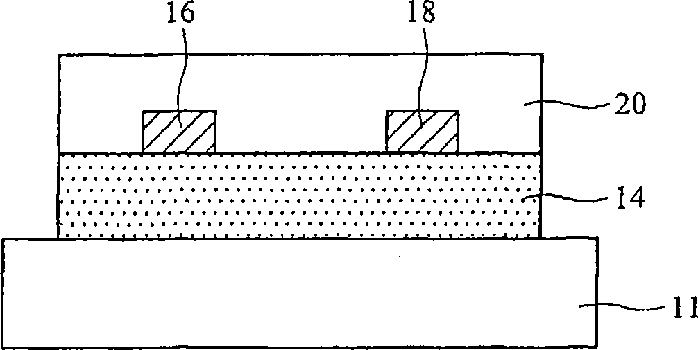
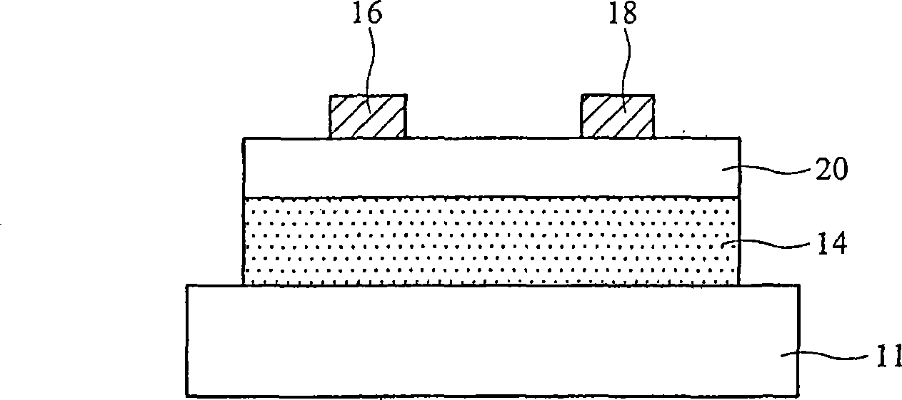
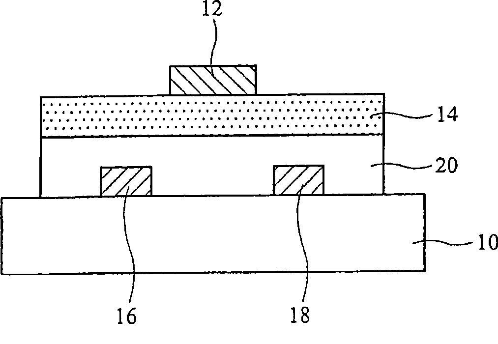
【Technical field】 [0001] The invention relates to an organic thin-film transistor, in particular to an organic thin-film transistor using a low-temperature cross-linkable polymer material as a dielectric layer, and the dielectric layer has adjustable surface energy. 【Background technique】 [0002] In recent years, compared with inorganic thin film transistors, organic thin film transistors (OTFTs) have the advantages of low process temperature and low cost for large displays. Therefore, the development of related materials and process technologies for OTFTs has gradually attracted attention. Pentacene or polythiophene with regioregularity is the most promising and competitive organic semiconductor material. [0003] However, for the gate dielectric layer in OTFT, SiO 2 Mainly, and the future development trend of OTFT must be based on comprehensive plasticization, so that OTFT can be produced using large-area and low-cost processes such as printing technology. Therefore, how...

Claims


Application Information

Patent Timeline
Patent Type & Authority Applications(China)
IPC IPC(8): H01L51/05H01L51/30H01L51/40C08L101/00C08J7/18
Inventor 杨丰瑜徐美玉
Owner IND TECH RES INST
Learn More