

Automatic control silicon chip check system
A technology for inspection systems and silicon wafers, used in semiconductor/solid-state device manufacturing, electrical components, semiconductor/solid-state device testing/measurement, etc. Less, reduce mechanical friction, reduce the effect of secondary pollution
- Summary
- Abstract
- Description
- Claims
- Application Information
AI Technical Summary
Problems solved by technology
Method used
Image

Examples
Embodiment Construction
[0030] The present invention will be described in detail below in conjunction with the accompanying drawings and embodiments.
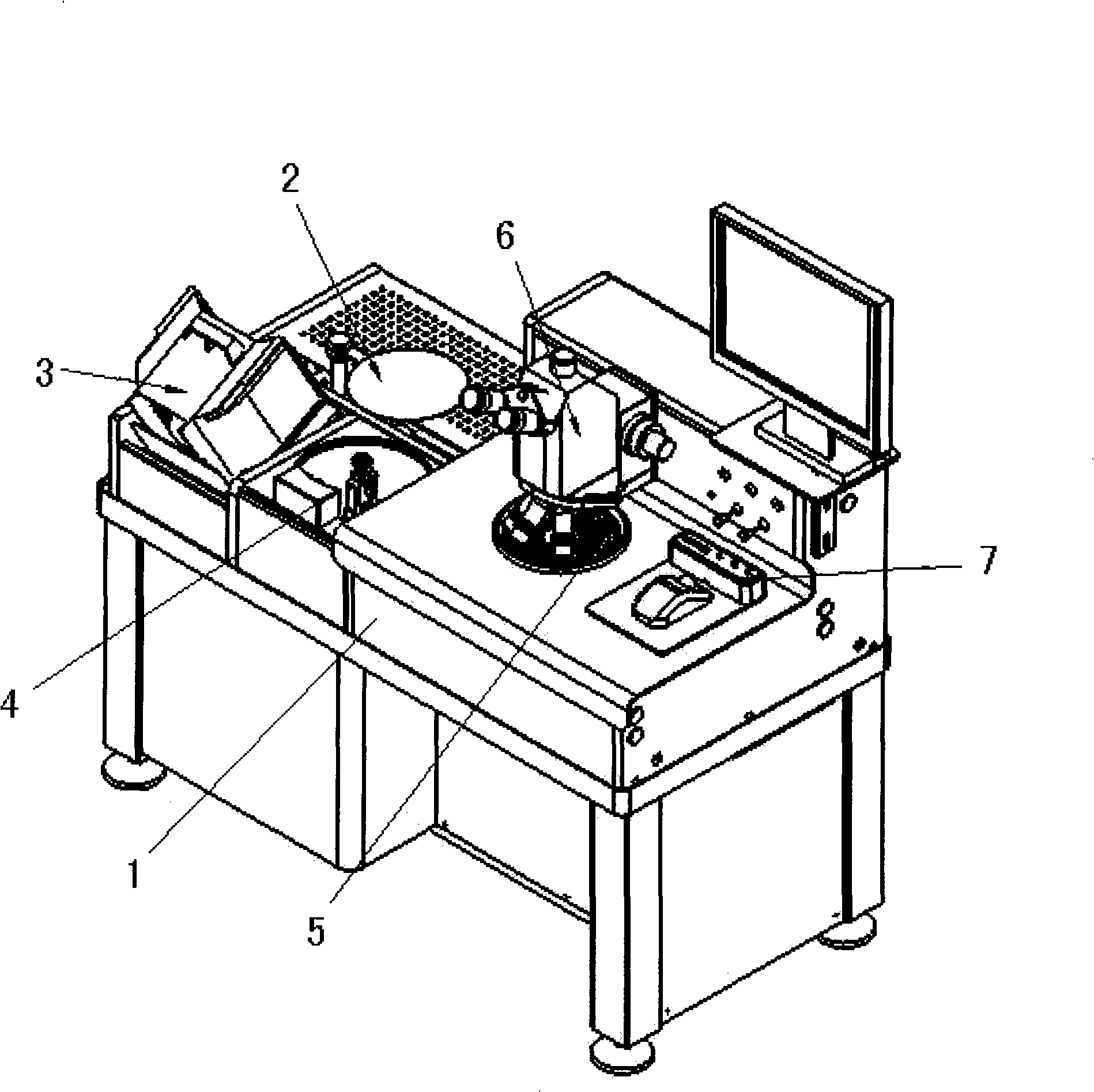
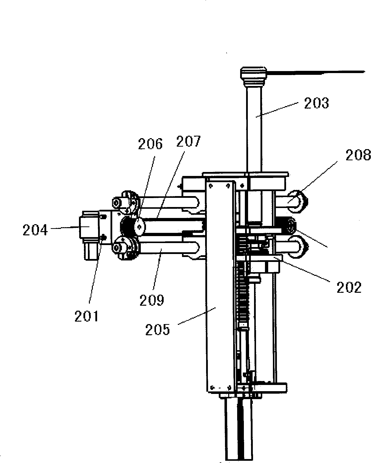
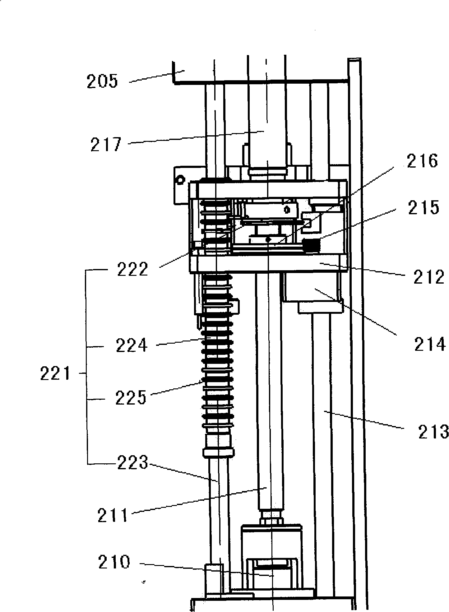
[0031] Such as figure 1 As shown, the present invention includes an operation table 1, on which a manipulator 2 for taking and delivering silicon wafers, a silicon wafer box platform 3 capable of tilting and swinging, and a silicon wafer surface inspection capable of spherical movement are arranged on the operating table 1. Mechanism 4, a rapidly positioned stage 5, a lens group 6 is arranged above the stage 5, and a computer control system 7 connected to the above-mentioned devices. These parts of the present invention all have independent operability, that is to say that these parts can be combined and applied to the present invention, and can also be used in other equipment alone, therefore, when a certain part involved in the present invention is applied to other occasions, Nor should it be excluded from the scope of protection described in the p...
PUM
 Abstract
Description
Claims
Application Information