Photovoltaic device containing nanoparticle sensitized carbon nanotubes

A photovoltaic device and nanoparticle technology, applied in nanotechnology, photovoltaic power generation, nanotechnology, etc., can solve problems such as high process temperature, inability to improve solar conversion efficiency, and low efficiency

Inactive Publication Date: 2009-04-15
SOLEXANT CORP (US)
View PDF0 Cites 13 Cited by
  • Summary
  • Abstract
  • Description
  • Claims
  • Application Information

AI Technical Summary

Problems solved by technology

The two main problems with CIGS solar cells are: (1) there is no clear path to higher efficiencies and (2) the high process temperatures make it difficult to use high speed roll to roll processes, so they cannot achieve significant low cost structure
However, polymers suffer from two major disadvantages: (1) inefficiency due to slow charge transport and (2) poor stability—especially to ultraviolet (UV) light
(See Furis et al., MRS Proceedings, volume 784, 2004) These techniques show improvements in photoluminescence, but cannot improve solar energy conversion efficiency since they cannot affect the charge transport properties of the hole transport layer and the electron transport layer

Method used


Image

  • Photovoltaic device containing nanoparticle sensitized carbon nanotubes
  • Photovoltaic device containing nanoparticle sensitized carbon nanotubes
  • Photovoltaic device containing nanoparticle sensitized carbon nanotubes

Examples


example 1

[0058] Figure 6 is a schematic diagram of an embodiment of a photosensitive nanoparticle sensitized carbon nanotube solar cell device pertaining to the present invention. By depositing a photoactive layer 630 comprising photoactive nanostructures comprising photoactive nanoparticle sensitized carbon nanotubes on a glass substrate layer 610 coated with a transparent conductive layer 620 such as ITO, followed by Depositing the cathode metal layer 640, the solar cell can be fabricated. The devices (610 to 640) or subsections of devices (such as 610, 620 and 630) are annealed at 200-400°C for 6-12 hours.

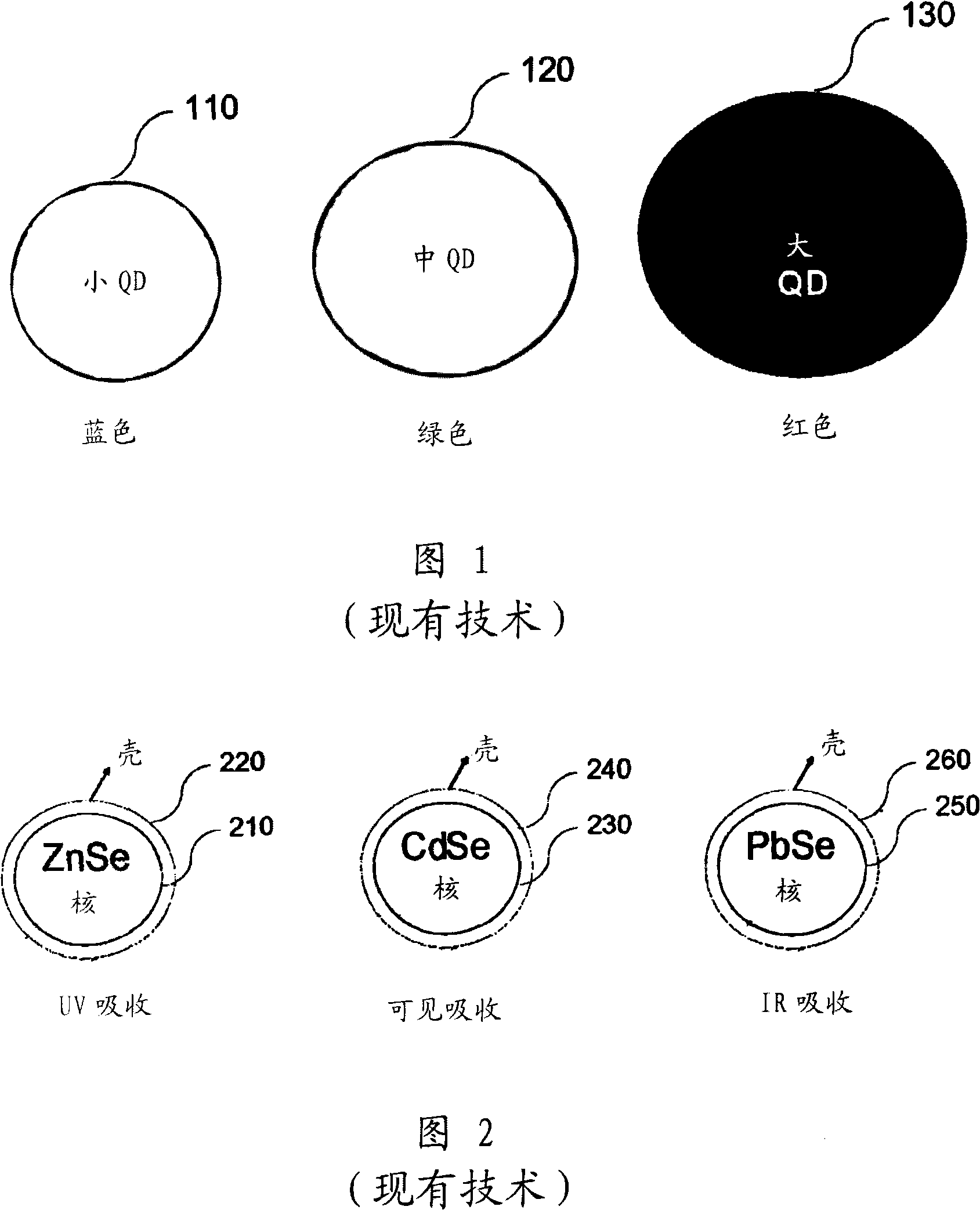
[0059] Photoactive nanoparticles can be made from Group IV, II-IV, II-VI and III-V materials. Some examples of photosensitive nanoparticles include Si, Ge, CdSe, PbSe, ZnSe, CdTe, CdS, PbS. The size of nanoparticles can be varied (eg: 2-10 nm) to obtain a range of bandgaps. These nanoparticles can be prepared according to methods known in the art. Nanoparticles can also be...

example 3

[0063] Figure 8 and Figure 9 Another embodiment using photosensitive nanoparticle-sensitized single-walled carbon nanotubes (SWCNTs) is shown in , wherein nanoparticle-sensitized SWCNT layers 830 or 940 are sandwiched between a SWCNT layer 840 (in Figure 8 in) or two SWCNT layers 930 and 950 (in Figure 9 middle). Photosensitive nanoparticle sensitized SWCNTs can be prepared using the method described in Example 1. By depositing a SWCNT layer 930 on a glass substrate 910 coated with a transparent conductor such as ITO 920, and then depositing a photoactive layer 940 on the SWCNT layer 930, followed by depositing a second SWCNT layer 950 and a metal layer 960, the Figure 9 The solar cell device shown in . The SWCNTs used in layers 930 and 950 can be optionally functionalized to render them soluble in suitable organic solvents and enhance their adhesion to other layers. Deposition of SWCNTs can be performed by spin coating or other molecular self-assembly methods known ...

example 4

[0066] exist Figure 11 In another embodiment shown in , the photoactive layer 1140 is sandwiched between two SWCNT layers. Figure 11 The solar cell device shown in can be fabricated by depositing a SWCNT layer on a glass substrate 1110 coated with a transparent conductor such as ITO 1120 . Photoactive nanoparticles are then deposited on top of SWCNT layer 1130 to form photoactive layer 1140, followed by deposition of second SWCNT layer 1150 and metal layer 1160. The device or subsection of the device is annealed at 200-400° C. for 6 to 12 hours. This results in a photoactive layer 1140 comprising photoactive nanoparticles alone or in combination with photoactive nanostructures comprising photoactive nanoparticles and n-type and / or p type SWCNT. In some cases, photoactive layer 1140 includes photoactive nanostructures made of photosensitive nanoparticles and p-type and / or n-type SWCNTs with little or no free nanoparticles present.

[0067] The SWCNTs used in layers 1130 a...


PUM


Abstract

This invention relates to photovoltaic devices made with photoactive nanostructures comprising carbon nanotubes and photosensitive nanoparticles.

Description

technical field [0001] The present invention relates to the use of carbon nanotubes and photoactive nanoparticles including nanoparticles of different sizes and compositions to form photovoltaic devices. Background technique [0002] Rising oil prices have increased the importance of renewable energy for economic development. Considerable efforts are being made worldwide to develop economical solar cells to harvest solar energy. Current solar technologies can be broadly classified into crystalline silicon and thin film technologies. More than 90% of solar cells are made of silicon - monocrystalline, polycrystalline or amorphous. [0003] Historically, crystalline silicon (c-Si) has been used as the light-absorbing semiconductor in most solar cells, although it is a relatively poor light-absorbing material and requires material of considerable thickness (hundreds of microns). However, it proves to be convenient because it gives stable solar cells with good efficiencies (12...

Claims


Application Information

Patent Timeline
Patent Type & Authority Applications(China)
IPC IPC(8): H01L51/42
CPCB82Y10/00H01L51/0037Y02E10/50H01L51/4213H01L51/0049H01L51/426H01L51/0036B82Y30/00Y02E10/549H10K85/113H10K85/1135H10K85/225H10K30/10H10K30/35H10K30/50H01L31/04H01L31/042
Inventor 达莫德·雷迪
Owner SOLEXANT CORP (US)
Why Eureka
Try Eureka