Semiconductor device
A semiconductor and terminal technology, applied in the direction of semiconductor devices, semiconductor/solid-state device components, electric solid-state devices, etc., can solve problems such as failure to fully correspond
- Summary
- Abstract
- Description
- Claims
- Application Information
AI Technical Summary
Problems solved by technology
Method used
Image

Examples
no. 1 Embodiment approach
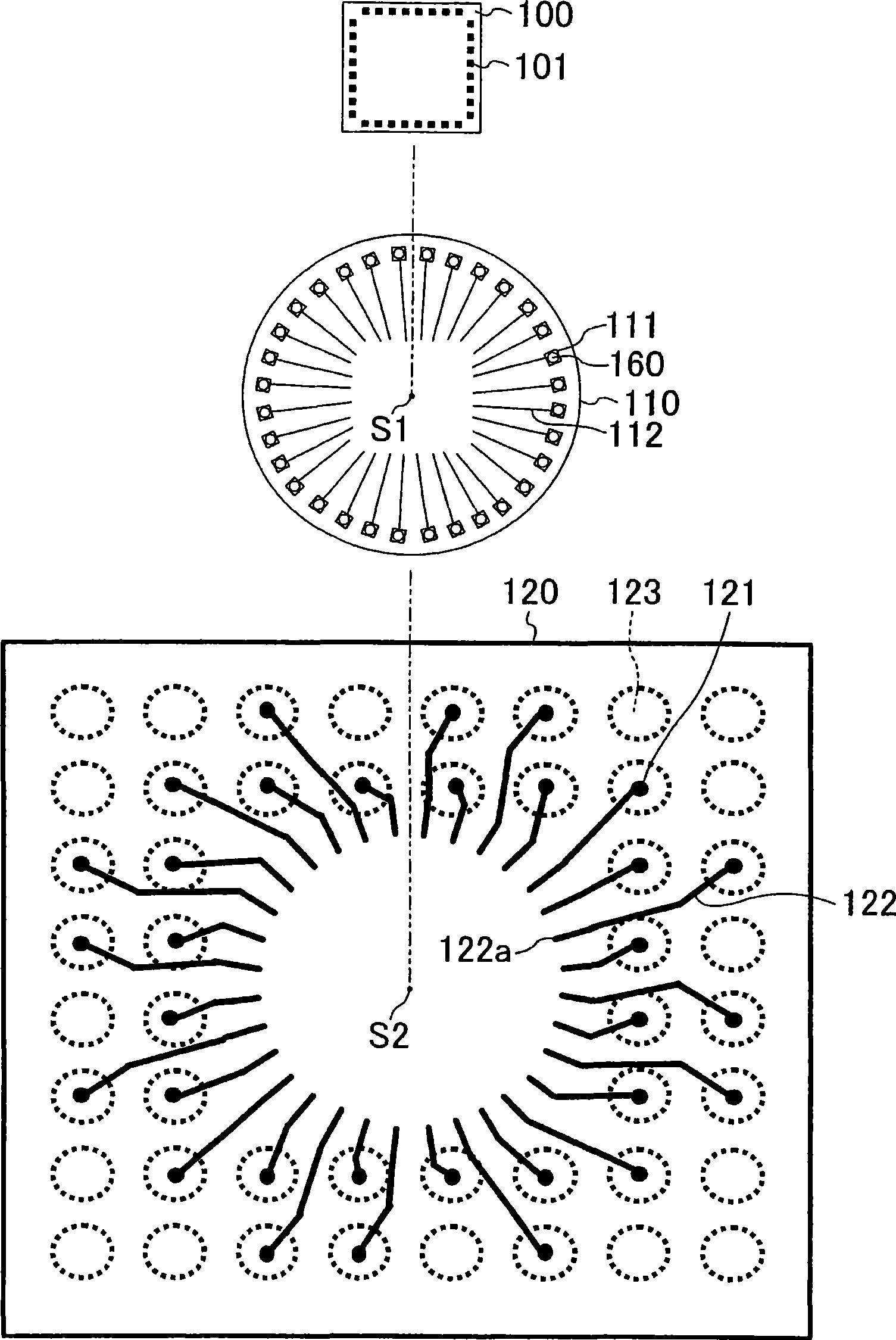
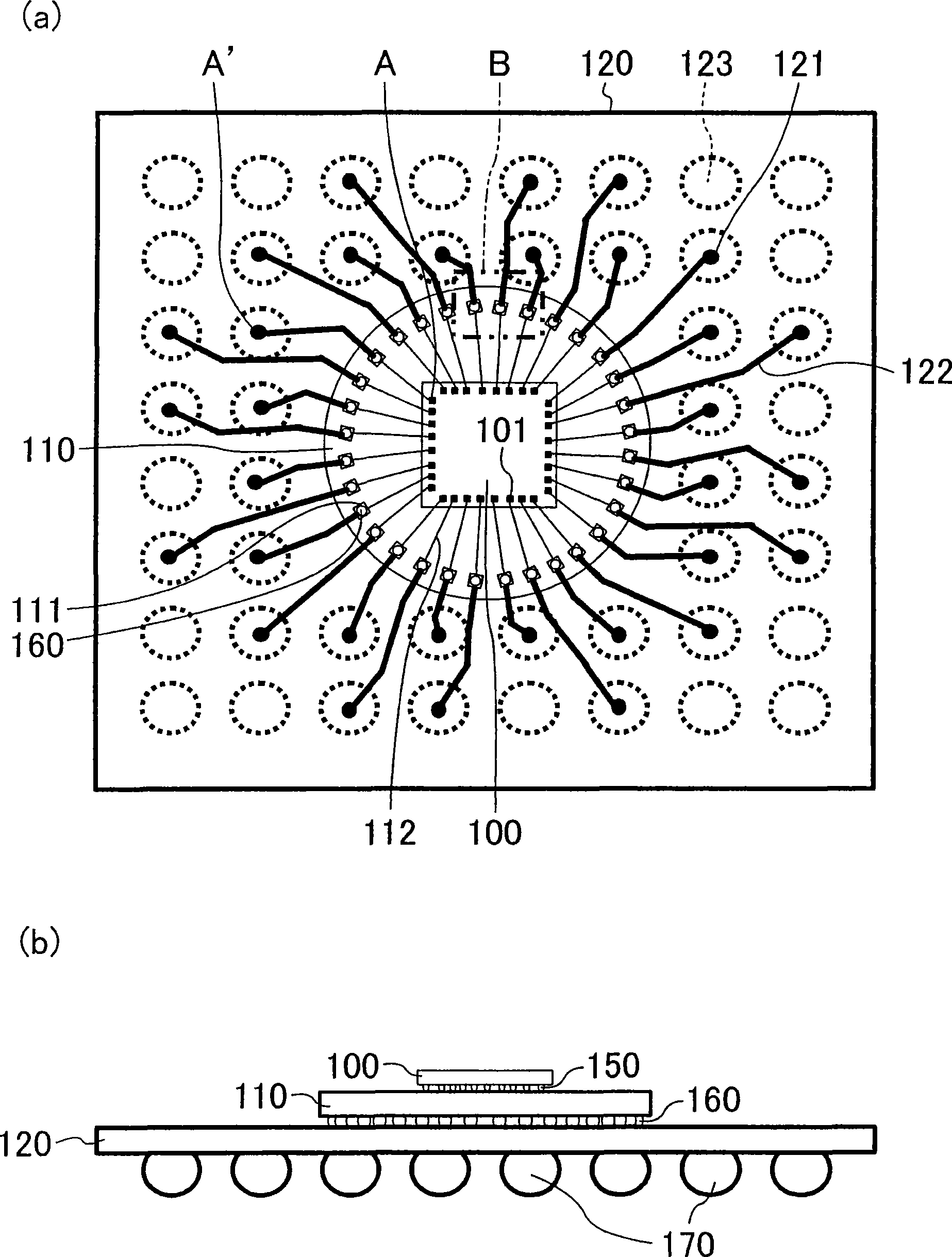
[0068] use figure 1 , figure 2 A~ figure 2 B. image 3 A~ image 3 C and Figure 4 , the semiconductor device in the first embodiment of the present invention will be described.
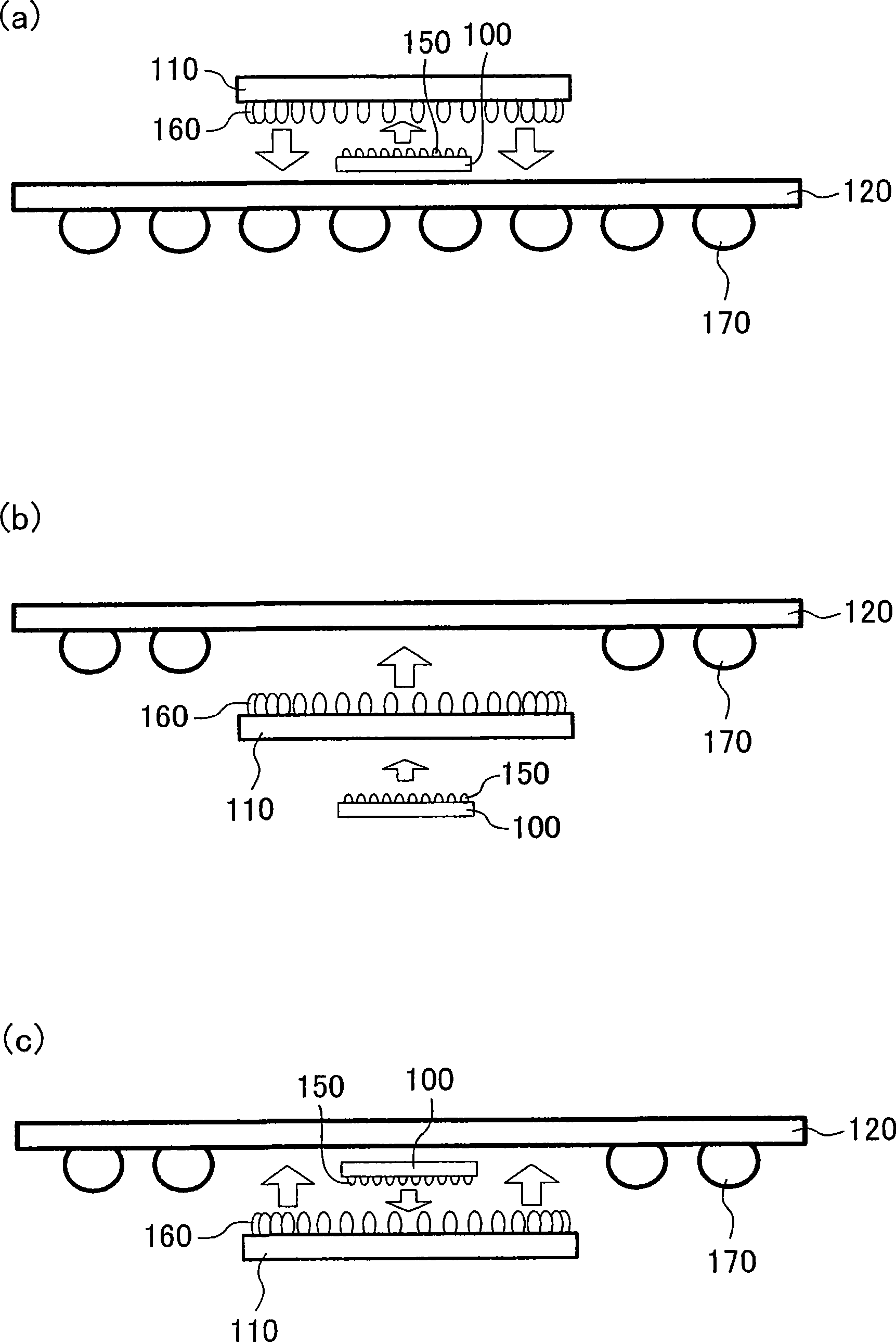
[0069] figure 1 It is an exploded plan view of the semiconductor device according to this embodiment. figure 2 A is a top view of a semiconductor device according to this embodiment, figure 2 B is a side view of the semiconductor device according to this embodiment. image 3 A~ image 3 C is with figure 2 A side view of a semiconductor device different from the semiconductor device shown in B. Figure 4 by taking the axis extending vertically with respect to the wiring group layer as the axis of rotation, from figure 2 The state of A is a top view of a semiconductor device that changes the state of the transmission target of a power signal and a signal other than the power signal (hereinafter, "signal of the power signal" is simply referred to as "signal") by turning the wiring group...
no. 2 Embodiment approach
[0092] In the second embodiment of the present invention, in the wiring group layer in the above-mentioned first embodiment, the signal terminals and the power supply terminals are separated from each other. Therefore, signal wiring and power supply wiring can be easily laid out in the wiring group layer. use Figure 5 A and Figure 5 B illustrates the semiconductor device in this embodiment mode. also, Figure 5 A is the bottom view of the wiring group layer, Figure 5 B is a top view of the substrate.
[0093] First, explain Figure 5 A and Figure 5 B's sign.
[0094] exist Figure 5 In A, 210 is a wiring group layer, 111a is a signal pad (second signal terminal) provided on the wiring group layer 210 , and 111b is a power pad (second power terminal) provided on the wiring group layer 210 . 215 is a wiring provided in the wiring group layer 210, and is a wiring that gathers the power supply pads 111b.
[0095] exist Figure 5 In B, 220 is a substrate, 123a is a s...
no. 3 Embodiment approach
[0101] In the third embodiment of the present invention, by changing the arrangement of vias connecting the wiring group layer and the substrate, it is possible to change the position where signals and power signals are output from the lower surface of the substrate compared to the first embodiment.
[0102] use Figure 6 A~6C and Figure 7 A semiconductor device according to this embodiment will be described. Figure 6 A~ Figure 6 C and Figure 7 yes figure 2 An enlarged plan view of area B shown in A. In addition, the connection method between the wiring group layer and the substrate, in Figure 7 In the figure, it is a wire bond (wire bond) connection, but in the present invention, a flip chip (filp chip) method may also be used.
[0103] First, explain Figure 6 A~ Figure 6 C and Figure 7 symbols in .
[0104] exist Figure 6 A~ Figure 6 C and Figure 7 Among them, 311 is a pad (second terminal) provided on the wiring group layer, 312 is a wiring (second ...
PUM
 Abstract
Description
Claims
Application Information
 - R&D Engineer
- R&D Manager
- IP Professional
- Industry Leading Data Capabilities
- Powerful AI technology
- Patent DNA Extraction
Browse by: Latest US Patents, China's latest patents, Technical Efficacy Thesaurus, Application Domain, Technology Topic.
© 2024 PatSnap. All rights reserved.Legal|Privacy policy|Modern Slavery Act Transparency Statement|Sitemap