

Production method of nano size air groove
A technology of nanometer size and manufacturing method, which is applied in the direction of nanostructure manufacturing, nanotechnology, nanotechnology, etc., can solve the problems of waveguide sidewall roughness and difficulty in making triangles, etc., and achieve the effect of solving the problem of sidewall roughness
- Summary
- Abstract
- Description
- Claims
- Application Information
AI Technical Summary
Problems solved by technology
Method used
Image

Examples
Embodiment Construction
[0032] In order to make the object, technical solution and advantages of the present invention clearer, the present invention will be described in further detail below in conjunction with specific embodiments and with reference to the accompanying drawings.
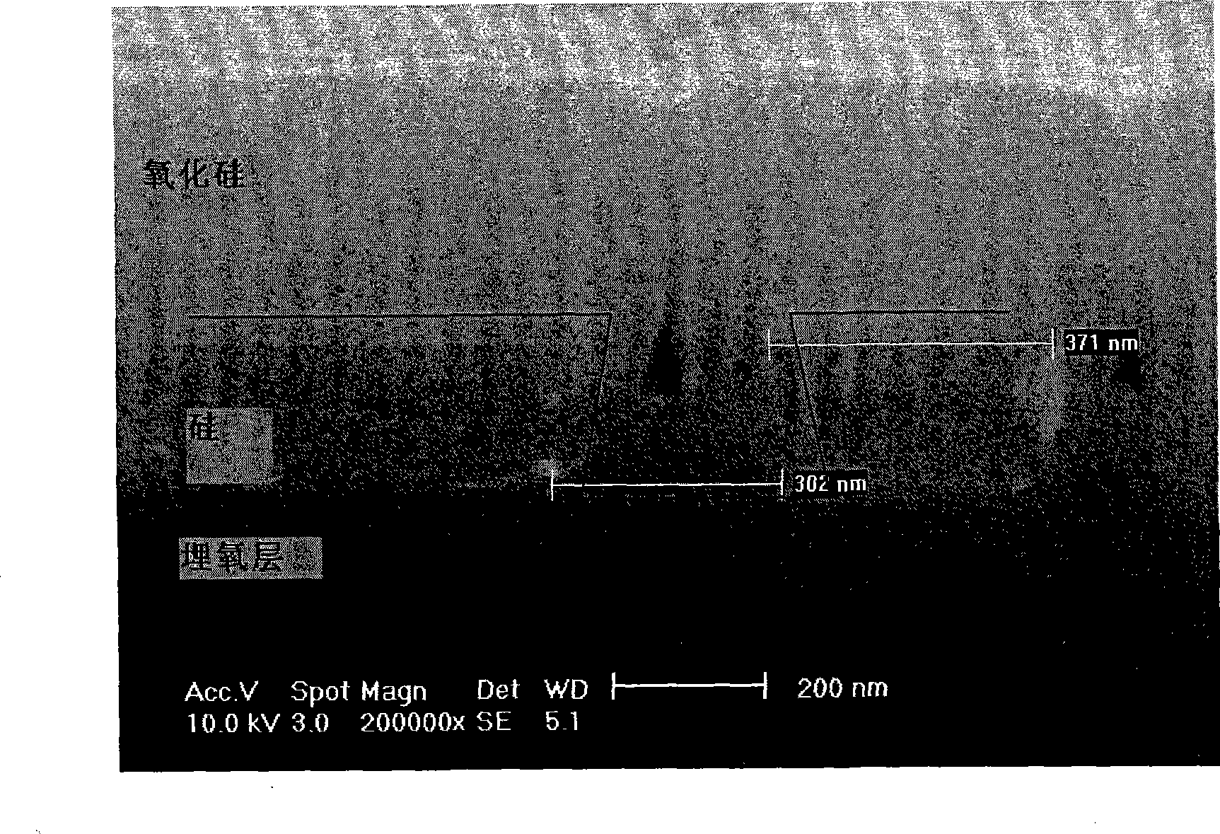
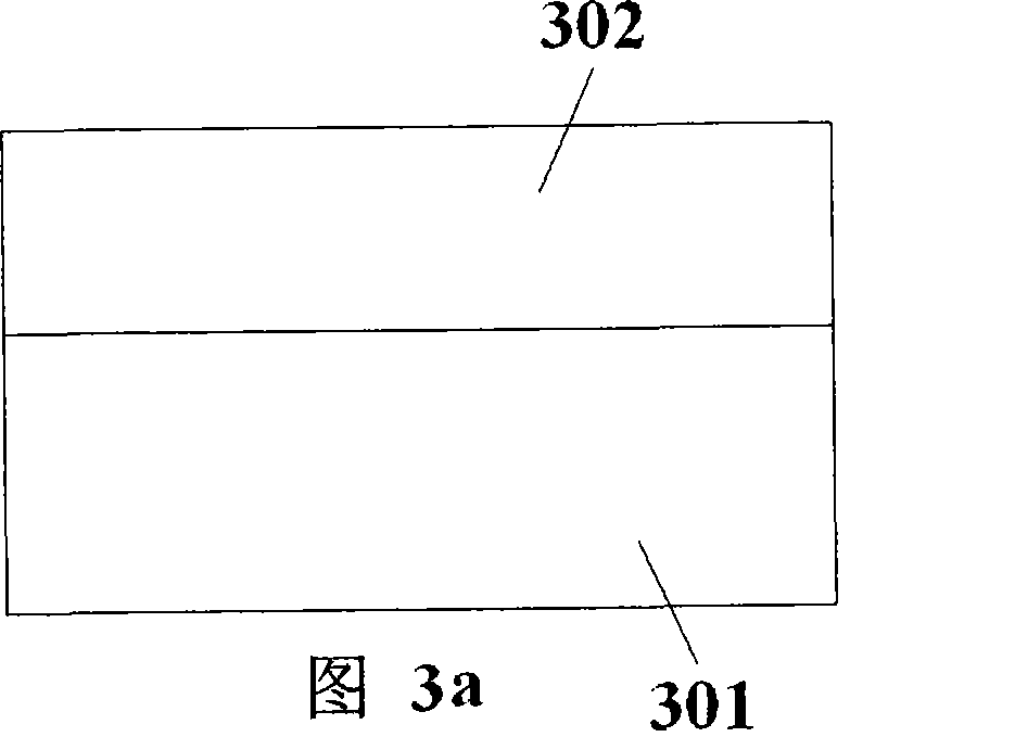
[0033] Fig. 3 is a schematic diagram of the steps of making an air groove by the method proposed by the present invention.
[0034] For the sake of clarity, in the description of this embodiment, the substrate material is silicon on insulator (SOI) as an example.
[0035] First, silicon-on-insulator (SOI) wafers are cleaned;
[0036] Next, as shown in FIG. 3a, a layer of electron beam photoresist 302 is coated on the cleaned silicon-on-insulator (SOI) sheet 301;
[0037] Then, as shown in Figure 3b, on the surface of the silicon-on-insulator (SOI) sheet, the exposure pattern is transferred to the electron beam photoresist by electron beam lithography technology. The shape of the exposure pattern is a rectangle, and the l...
PUM
| Property | Measurement | Unit |
|---|---|---|
| Thickness | aaaaa | aaaaa |
Abstract
Description
Claims
Application Information