Semiconductor laser welding method

A laser welding and semiconductor technology, used in laser welding equipment, welding equipment, metal processing equipment, etc., can solve the problems of inability to weld, the welding effect cannot meet the ideal requirements, and the bending of tin wires, so as to improve the welding quality and improve the solder joints. Adhesion and welding success rate, the effect of reducing welding defects

Active Publication Date: 2009-05-13
深圳市大族微加工软件技术有限公司
View PDF0 Cites 6 Cited by
  • Summary
  • Abstract
  • Description
  • Claims
  • Application Information

AI Technical Summary

Problems solved by technology

[0004] However, this control method is relatively simple. In practical applications, due to the difference in materials and the individuation and specialization of workpieces, the welding effect is far from meeting the ideal requirements.
For example, in the process of soldering, due to improper modulation of laser power, the tin wire is often bent, or the tin wire melts into beads and cannot be welded. Similar phenomena will also occur in the welding of other single crystal materials.

Method used


Image

  • Semiconductor laser welding method
  • Semiconductor laser welding method

Examples


Embodiment Construction

[0026] In order to make the objectives, technical solutions and advantages of the present invention clearer, the following further describes the present invention in detail with reference to the accompanying drawings and embodiments. It should be understood that the specific embodiments described herein are only used to explain the present invention, but not to limit the present invention.
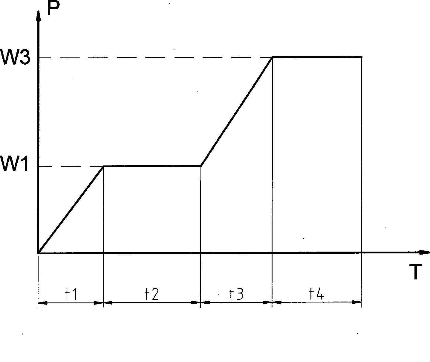
[0027] The core idea of ​​the method for improving the welding process of a semiconductor laser machine in the embodiment of the present invention is: based on the material characteristics of the sample itself, the melting point curve and the welding point curve of the material to be welded are established, and the maximum welding point adhesion is the goal. The welding process has been improved.

[0028] Such as figure 1 As shown, the welding process of the embodiment of the present invention is formulated according to the following steps:

[0029] Step A. Establish melting point characteris...


PUM


Abstract

The invention discloses a semiconductor laser welding method, the welding method includes the following four stages: the temperature rising stage, in which the laser power gradually rises from zero and the temperature of the welding flux rises the melting point or the approximate melting point from the room temperature; the maintaining stage, in which the laser power maintains invariable or slightly rises upon the laser power W1 at the later stage of rising the temperature; melting stage, in which the laser power continuously rises based on the later maintaining stage so that the welding flux is fully melted or close to the full melting; and the subsequent stage, in which the laser power maintains invariable upon the laser power W3 at the later melting stage so as to achieve welding. The invention has the advantages that work pieces can be optimized by processing parameters, the adhesive force of the samples to the welding point is greatly enhanced, wherein, the welding success rate for the tin soldering at one time reaches 100%, the situations such as false welding, lack welding, unsoldering and the like are not generated, and the oxidation phenomenon of the welded work pieces can be effectively avoided. Therefore, the continuous welding of the plastic welding can be realized to avoid the phenomenon for the initial point, the end point and the focal point, and the intensity of the welding point can surpass that of the original materials.

Description

[Technical Field] [0001] The invention relates to laser welding technology, in particular to a semiconductor laser welding method. [Background technique] [0002] Semiconductor laser welding is currently a cutting-edge laser welding technology. Its main features are good beam quality, high photoelectric conversion efficiency, small size of the equipment, simple maintenance, etc. It is used for welding low melting point materials (such as soldering, In plastic welding), it has a broad application foundation and development prospects. [0003] At present, most of the semiconductor laser welding methods are continuous laser welding with "gradual and gradual output", which is characterized by eliminating the "flares" caused by sudden current changes when the semiconductor is instantly pressurized; at the same time, it is beneficial to improve the life of the semiconductor laser. [0004] However, this control method is relatively single. In practical applications, due to the differen...

Claims


Application Information

Patent Timeline
IPC IPC(8): B23K26/20B23K26/40B23K26/21B23K26/22
CPCB23K26/203B23K26/211
Inventor 高云峰姜钧陆业钊倪明生陈玩林
Owner 深圳市大族微加工软件技术有限公司
Why Eureka
Try Eureka