

Plasma confinement apparatus and semiconductor processing equipment applying the same
A plasma and confinement device technology, applied in the field of microelectronics, can solve problems such as complicated installation and maintenance, complicated installation and positioning, and complicated mechanical connection, and achieve the effects of convenient installation and maintenance, prolonging service life, and avoiding particle pollution
- Summary
- Abstract
- Description
- Claims
- Application Information
AI Technical Summary
Problems solved by technology
Method used
Image

Examples
Embodiment Construction
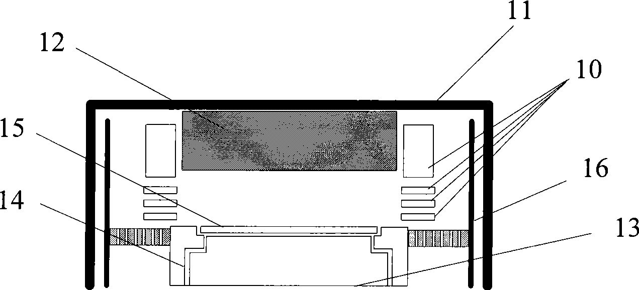
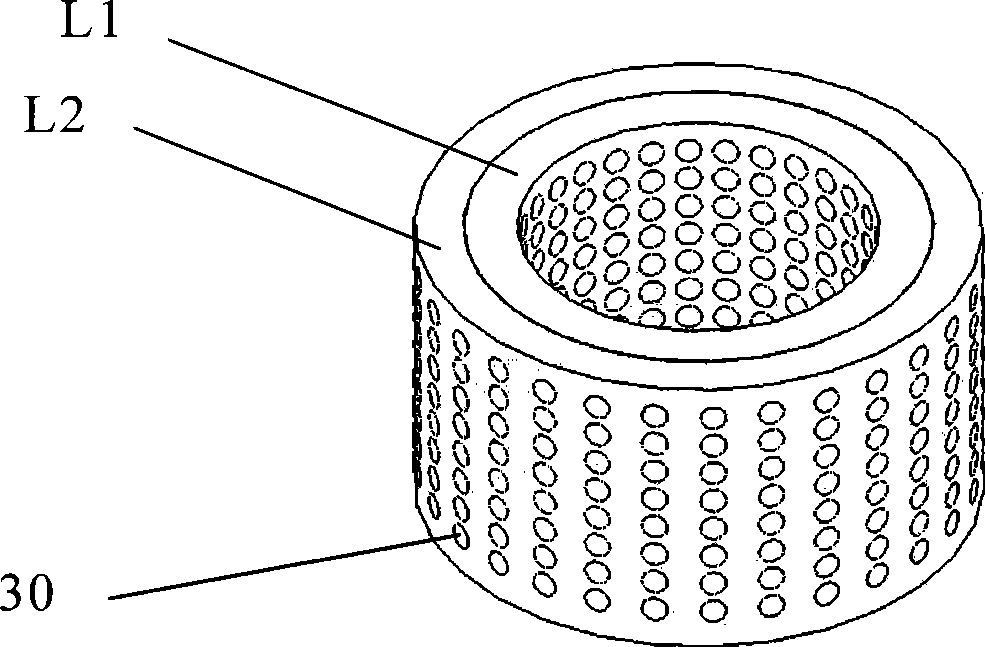
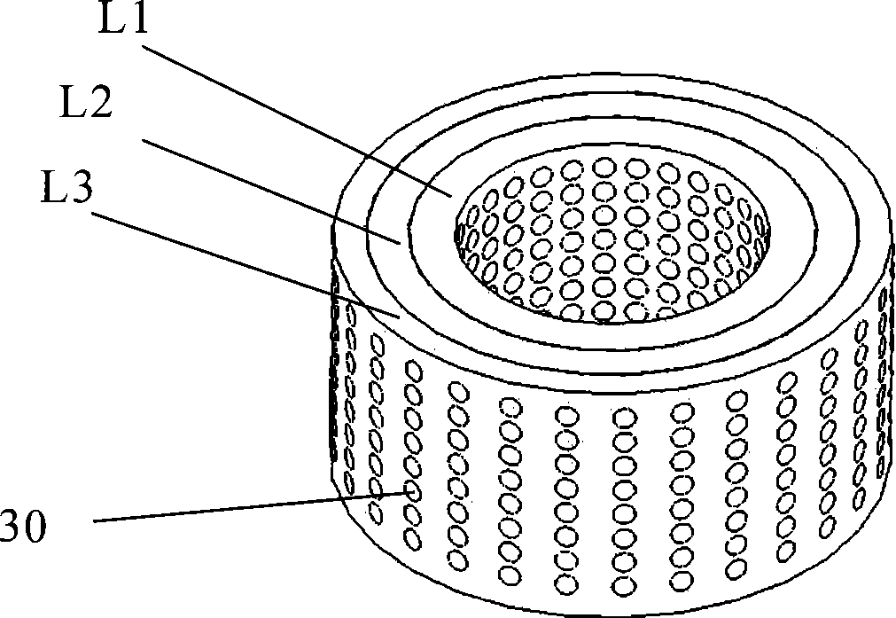
[0044] The technical core of the plasma confinement device provided by the present invention and the semiconductor processing equipment using the plasma confinement device is to set at least one layer of cylindrical plasma confinement cover, and open a through hole on it to form a hole that penetrates the confinement device. The walls confine the channel so that the plasma cannot diffuse beyond the confines of the plasma confinement enclosure. The confinement shield mentioned in the present invention refers to each layer of cylindrical structure surrounding the reaction area to restrict the outward movement (eg, diffusion movement) of the plasma in the area. In the present invention, a single-layer confinement cover can be used to form the plasma confinement device for restricting the outward movement of plasma alone, or multiple layers of confinement cover can be combined to form the plasma confinement device.
[0045] In order to enable those skilled in the art to better und...
PUM
 Abstract
Description
Claims
Application Information