Photosensor and display device
A light sensor and display device technology, applied in radiation control devices, instruments, optics, etc., can solve the problem of difficulty in obtaining a large number of light signals, and achieve the effect of increasing sensitivity
- Summary
- Abstract
- Description
- Claims
- Application Information
AI Technical Summary
Problems solved by technology
Method used
Image
Examples
no. 1 example
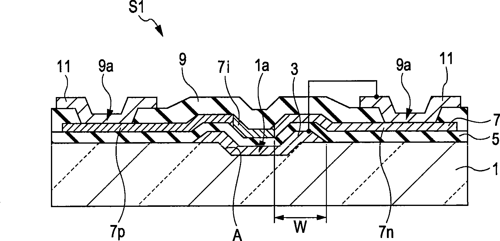
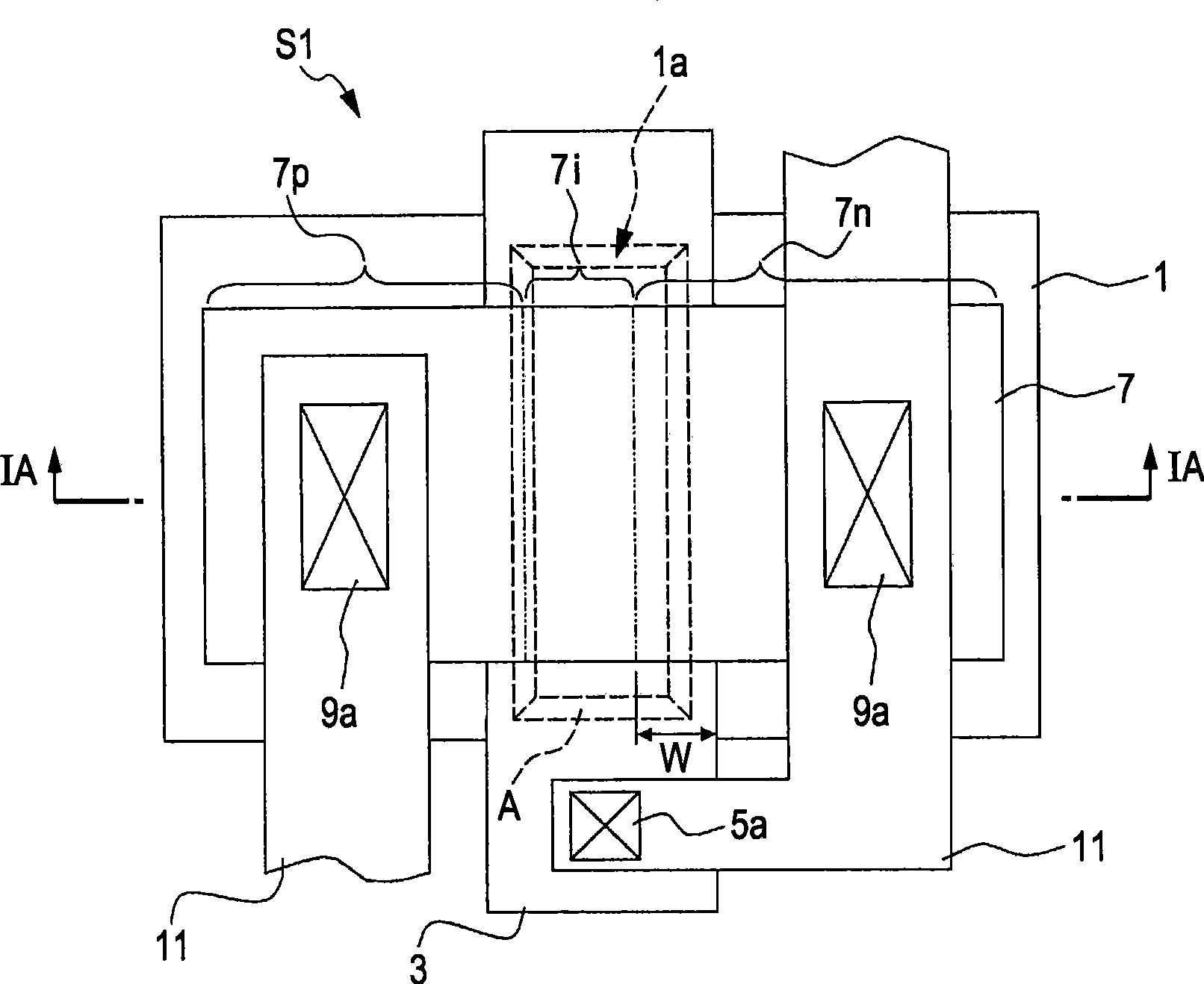
[0031] Figure 1A is a schematic sectional view of a substantial part of the photosensor S1 which is a feature of the display device according to the first embodiment of the present invention. Figure 1B is the plan view of light sensor S1. Figure 1B The cross-section taken along line IA-IA corresponds to Figure 1A shown.
[0032] The photosensor S1 is a photosensor S having a so-called PIN thin film diode structure. The photosensor S1 has the following structure.
[0033] A substrate 1 made of a transparent material has a groove 1a on one surface. The groove 1 a has a forward tapered sloped side wall A whose groove width gradually increases toward the opening end of the groove.
[0034] A reflective material layer 3 made of light reflective material is patterned on the substrate 1 to cover the inner walls, including the bottom and inclined side walls A and the periphery of the groove 1a. It is important that the reflective material layer 3 has a thickness not filling ...
no. 2 example
[0063] image 3 is a plan view of a photosensor S2 which is a feature of a display device according to a second embodiment of the present invention. along image 3 The section intercepted by the IA-IA line is the same as the Figure 1A same as shown in .
[0064] The photosensor S2 differs from the photosensor S1 according to the first embodiment in that the photosensor S2 has a plurality of grooves 1 a in the substrate 1 . Other structures of the optical sensor S2 are the same as those of the optical sensor S1.
[0065] In this case, all the grooves 1 a are arranged below the portion of the light receiving portion (i region) 7 i provided with the semiconductor thin film 7 . The shape of each groove 1a is the same as that in the first embodiment. In other words, each groove 1a has a forward tapered inclined side wall A, wherein the width of the groove gradually increases toward the opening end of the groove. The reflective material layer 3 is configured to completely cov...
no. 3 example
[0070] Figure 4A is a schematic cross-sectional view of a photosensor S3, which is a feature of a display device, according to a third embodiment of the present invention. Figure 4B is a plan view of light sensor S3. along Figure 4B The section taken by the IVA-IVA line corresponds to Figure 4A shown.
[0071] Figure 4A and Figure 4BThe photosensor S3 shown differs from the photosensor S1 according to the first embodiment in that the reflective material layer 3 is connected to the p region 7p of the semiconductor thin film 7 . Other structures of the optical sensor S3 are the same as those of the optical sensor S1, including the lamination relationship between the groove 1a, the reflective material layer 3 and the semiconductor thin film 7.
[0072] In the photosensor S3 having the above-mentioned structure, the reflective material layer 3 is arranged on the bottom and the inclined side wall A of the groove 1a of the substrate 1, so that the orientation of the disp...
PUM
| Property | Measurement | Unit |
|---|---|---|
| thickness | aaaaa | aaaaa |
Abstract
Description
Claims
Application Information
 - R&D
- Intellectual Property
- Life Sciences
- Materials
- Tech Scout
- Unparalleled Data Quality
- Higher Quality Content
- 60% Fewer Hallucinations
Browse by: Latest US Patents, China's latest patents, Technical Efficacy Thesaurus, Application Domain, Technology Topic, Popular Technical Reports.
© 2025 PatSnap. All rights reserved.Legal|Privacy policy|Modern Slavery Act Transparency Statement|Sitemap|About US| Contact US: help@patsnap.com


