Method for preparing crystalline silicon solar cell with passivation on double surfaces

A solar cell and double-sided passivation technology, which is applied in the field of solar photovoltaic utilization, can solve the problems of large-scale, low-cost industrial production of solar cells, and high price, so as to be suitable for large-scale production, improve conversion efficiency, reduce small bend effect

Inactive Publication Date: 2009-06-03
上海晶澳太阳能光伏科技有限公司
View PDF0 Cites 49 Cited by
  • Summary
  • Abstract
  • Description
  • Claims
  • Application Information

AI Technical Summary

Problems solved by technology

Due to the use of photolithography, laser and other equipment, it is expensive and not suitable for large-scale and low-cost industrial production of solar cells

Method used


Image

  • Method for preparing crystalline silicon solar cell with passivation on double surfaces
  • Method for preparing crystalline silicon solar cell with passivation on double surfaces
  • Method for preparing crystalline silicon solar cell with passivation on double surfaces

Examples


Embodiment Construction

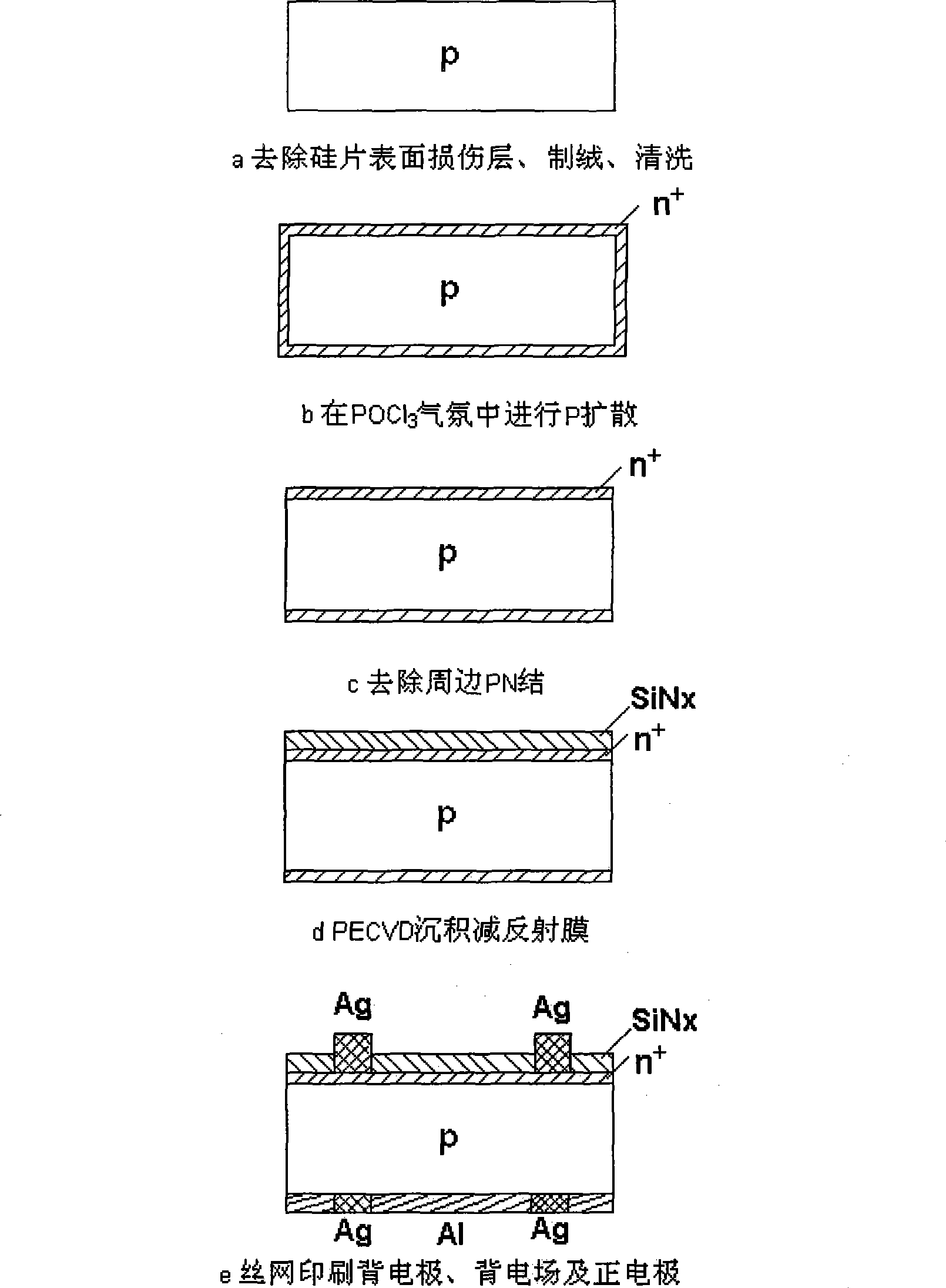
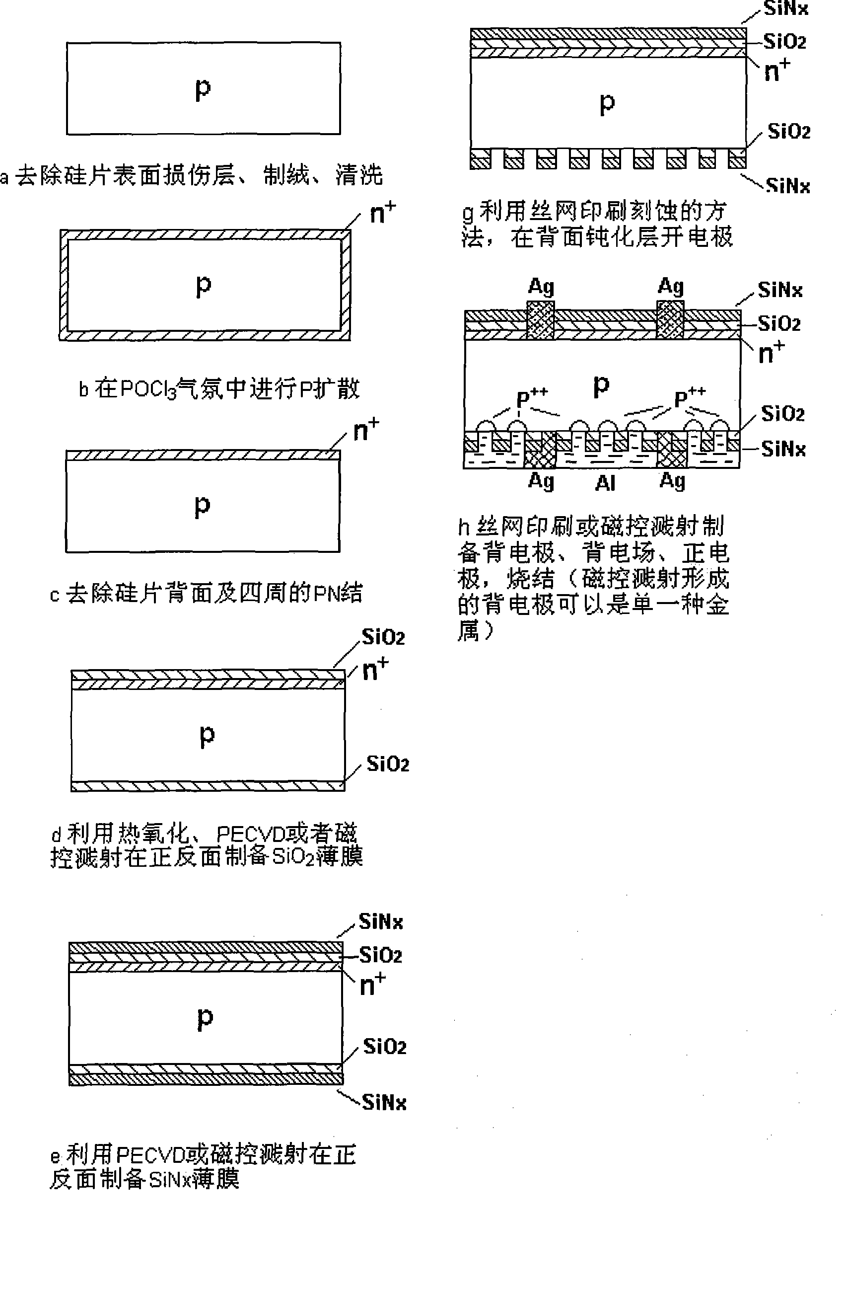
[0030] The present invention will be further described below in conjunction with the accompanying drawings and embodiments. figure 2 Shown is the specific preparation process of the double-sided passivated crystalline silicon solar cell of the embodiment of the present invention:

[0031] (1) Remove the damaged layer and the textured surface of the silicon wafer surface;

[0032] (2) Diffusion of P in POCl3 atmosphere to form n + diffusion layer;

[0033] (3) Use wet etching to remove the PN junction on the back of the silicon wafer and the surrounding area (the traditional process only needs to remove the PN junction around the silicon wafer after diffusion, and the PN junction on the back side will be removed during the process of making the back electric field. A1 is compensated, but in the process of preparing double-sided passivated solar cells, since the aluminum paste printed on the back will be separated by the laminated passivation layer, it cannot compensate for t...


PUM


Abstract

The invention discloses a method for preparing a crystalline silicon solar cell with passivation on double surfaces. The method comprises the following steps: laminated passivation layers are prepared on the front and the back surfaces of the solar cell; by utilizing a method of screen printing corrosive sizing agent on the laminated passivation layer on the back surface, an electrode window is opened on the laminated passivation layer on the back surface; and then a back electrode is formed by screen printing or sputtering on the electrode window. By utilizing the screen printing corrosive sizing agent method, a structure of passivation on double surfaces of the solar cell is achieved; the structure greatly improves long-wave responses of the solar cell, and increases the conversion efficiency of the solar cell; and meanwhile, as an all-aluminium back surface field is cancelled and a local aluminum back surface field is adopted, bending of the solar cell is reduced and the structure is more suitable for the trend of solar cell thin section. As the method utilizes screen printing technique to replace pholithography and a laser sintering method, production costs are saved. Furthermore, the method is more suitable for mass production.

Description

technical field [0001] The invention relates to the field of photovoltaic utilization of solar energy, in particular to a preparation method of a crystalline silicon solar cell. Background technique [0002] The current commercial solar cell production process is simple and the manufacturing cost is relatively low. Its production process is as figure 1 Shown: Remove the damaged layer on the surface of the silicon wafer, make the textured surface → in POCl 3 Diffusion of P in the atmosphere to form n + Diffusion layer → use plasma etching or wet etching to remove the PN junction around the silicon wafer → use PECVD technology to deposit SiNx anti-reflection film on the front → screen print the back electrode, back electric field, and positive electrode → form by sintering in a sintering furnace Ohmic contact → test sorting. This commercial solar cell manufacturing technology is relatively simple, low in cost, suitable for industrialized and automated production, and thus ...

Claims


Application Information

Patent Timeline
Patent Type & Authority Applications(China)
IPC IPC(8): H01L31/18
CPCY02P70/50
Inventor 陶龙忠邢国强
Owner 上海晶澳太阳能光伏科技有限公司
Why Eureka
Try Eureka