CuInSe2-based thin film solar cell

A solar cell, cuinse2-ysy technology, applied in the field of solar cells, can solve the problems of insufficient utilization rate of incident light and limited contribution of device conversion efficiency, etc.

Inactive Publication Date: 2010-11-10
普尼太阳能(杭州)有限公司
View PDF3 Cites 2 Cited by
  • Summary
  • Abstract
  • Description
  • Claims
  • Application Information

AI Technical Summary

Problems solved by technology

[0016] 1. Due to the effect of elements such as Ga and S on CuInSe 2 The influence of the electronic band structure of thin film materials is different. The method of gradually changing the composition of a single element can only improve the collection efficiency of one kind of carrier, and the contribution to the conversion

Method used


Image

  • CuInSe2-based thin film solar cell
  • CuInSe2-based thin film solar cell
  • CuInSe2-based thin film solar cell

Examples


Embodiment 1

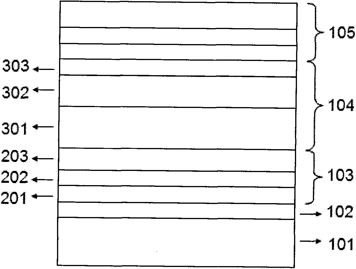
[0063] Such as figure 1 As shown, a CuInSe 2 The base thin-film solar cell is composed of a glass substrate 101 , a Mo thin-film electrode 102 , a reflective layer 103 , a photoelectric conversion layer 104 and a transparent conductive layer 105 in sequence.

[0064] The glass substrate 101 is made of soda-lime glass, and the Mo thin-film electrode 102 is deposited on the glass substrate 101 by magnetron sputtering. The thickness of the Mo thin-film electrode 102 is 1 μm, and the sheet resistance is 0.1-0.2Ω / □.

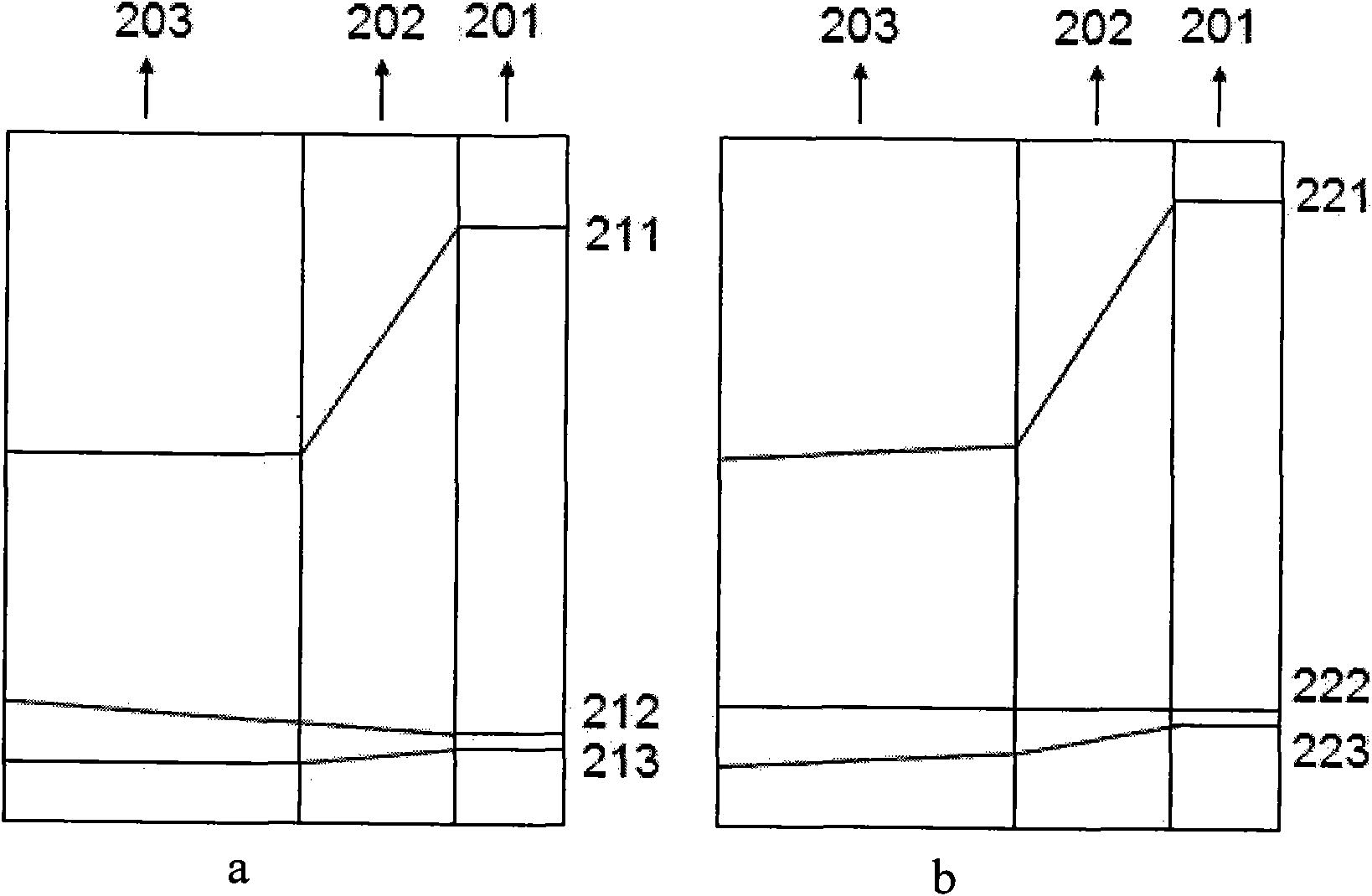
[0065] Such as figure 2 As shown, the reflective layer 103 is made of CuAlSe 2 / CuAl x Ga 1-x Se 2 / CuGaSe 2 The films are sequentially formed, among which, CuAlSe 2 The thickness of the film 201 is 10nm; CuAl x Ga 1-x Se 2 The thickness of the film 202 is 15nm; CuGaSe 2 Thin film 203 has a thickness of 25 nm.

[0066] In the reflective layer 103, CuAlSe 2 Thin film 201 is a p-type semiconductor thin film material, and its carrier concentration is 5×10 ...

Embodiment 2

[0089] Same as Example 1, except:

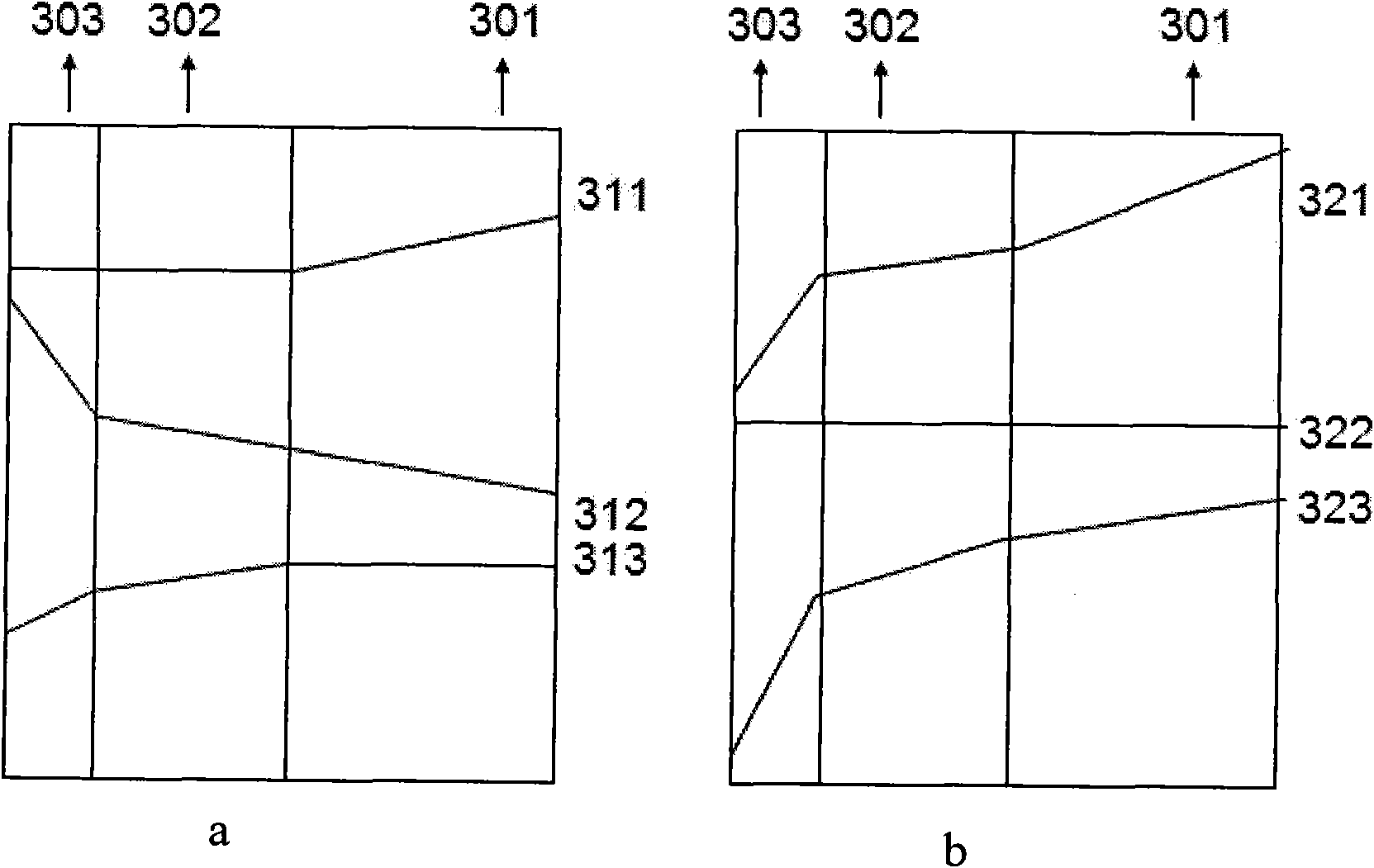
[0090] CuAlSe 2 The thickness of film 201 is 15nm, CuAl x Ga 1-x Se 2 The thickness of the thin film 202 is 20nm, CuGaSe 2 The thickness of the film 203 is 30nm; CuIn x Ga 1-x Se 2 Thickness of film 301 is 750nm; CuInSe 2-x S x The thickness of film 302 is 550nm; Cu 1-y Zn y InSe 2-x S x The thickness of the film 303 is 100nm; the thickness of the CdS film is 50nm, the thickness of the i-ZnO film is 60nm, and the thickness of the AZO film is 800nm.

[0091] CuInSe of this embodiment 2 The photoelectric conversion efficiency of the base thin film solar cell can reach more than 23% under standard irradiation conditions.

Embodiment 3

[0093] Same as Example 1, except:

[0094] CuAlSe 2 The thickness of the film 201 is 20nm, CuAl x Ga 1-x Se 2 The thickness of the film 202 is 50nm, CuGaSe 2 The thickness of the film 203 is 20nm; CuIn x Ga 1-x Se 2 Thickness of film 301 is 850nm; CuInSe 2-x S x The thickness of film 302 is 450nm; Cu 1-y Zn y InSe 2-x S x The thickness of the film 303 is 120nm; the thickness of the CdS film is 70nm, the thickness of the i-ZnO film is 70nm, and the thickness of the AZO film is 650nm.

[0095] CuInSe of this embodiment 2 The photoelectric conversion efficiency of the base thin film solar cell can reach more than 22% under standard irradiation conditions.


PUM

PropertyMeasurementUnit
Thicknessaaaaaaaaaa
Thicknessaaaaaaaaaa
Thicknessaaaaaaaaaa

Abstract

The invention discloses a CuInSe2-based thin film solar cell, which comprises a substrate, a metal anode, a reflecting layer, a photoelectric conversion layer and a transparent conductive layer in sequence, wherein the reflecting layer comprises CuAlSe2/CuAlxGa(1-x)Se2/CuGaSe2 films in sequence; the photoelectric conversion layer comprises CuIn(1-m)GamSe2/CuInSe(2-y)Sy/Cu(1-a)ZnaInSe(2-b)Sb films; and the transparent conductive layer comprises CdS/i-ZnO/AZO films. In the invention, the photoelectric conversion layer and the reflecting layer are constructed by adopting multilayer film and gradient film technologies; and a better p-n energy band structure can be formed by adjusting and controlling the bottom of a conduction band and a value band edge through interlayer charge migration, so that the long wave response of devices and the collection efficiency of current carriers can be improved and further the photoelectric conversion efficiency of the devices can be improved.

Description

technical field [0001] The invention belongs to the technical field of solar cells, in particular to CuInSe 2 based thin film solar cells. Background technique [0002] At present, commercialized solar cells mainly include: silicon-based wafer cells, thin-film solar cells and gallium arsenide-based concentrator solar cells, among which CuInSe 2 Because of its low production cost, high conversion efficiency, good low-light performance, strong radiation resistance, no light-induced degradation, and the ability to deposit on flexible substrates, thin-film solar cells are internationally known as "the most promising solar cell in the next era." Promising new thin-film solar cells". [0003] CuInSe 2 The structural development of base thin-film solar cells has mainly gone through three stages. In 1976, Kazmerski and others prepared the first CuInSe 2 Thin film solar cell, its structure is: glass substrate / Mo electrode / low resistance CuInSe 2 / High resistance CuInSe 2 / hig...

Claims


Application Information

Patent Timeline
IPC IPC(8): H01L31/042H01L31/065H01L31/0352H01L31/068H01L31/078
CPCY02E10/52Y02E10/547
Inventor 张晓勇王东李学耕
Owner 普尼太阳能(杭州)有限公司
Why Eureka
Try Eureka