Quartz wafer deep micropore processing equipment and method

A technology for processing quartz wafers and microholes, which is applied in the direction of microlithography exposure equipment, chemical instruments and methods, microstructure technology, etc., can solve the problem of charged particles charged by ion drilling, which cannot be solved well, and cannot be solved by quartz wafers. Processing of micro-holes, failure to meet the requirements of micro-electro-mechanical systems, etc., to achieve the effect of fast etching speed, easy implementation, and low cost

Inactive Publication Date: 2009-06-10
INST OF MICROELECTRONICS CHINESE ACAD OF SCI
View PDF0 Cites 5 Cited by
  • Summary
  • Abstract
  • Description
  • Claims
  • Application Information

AI Technical Summary

Problems solved by technology

[0003] However, the excellent characteristics of quartz make it more and more widely used in the manufacture of MEMS. Due to the selectivity of the etching method, it is impossible to etch microholes on quartz, and because of the light transmission, it is not suitable for laser drilling. also impossible
[0004] At present, the minimum aperture of ultrasonic drilling is about 0.3mm, which is far from meeting our requirements in the micro-fabrication of micro-electromechanical systems (MEMS), and ion drilling cannot be well solved due to the charge problem of charged particles.
[0005] Therefore, the above-mentioned various micropore processing methods cannot process micropores that meet the requirements on the quartz wafer very well.
Especially the processing of deep micro-holes on quartz wafers is more difficult

Method used


Image

  • Quartz wafer deep micropore processing equipment and method
  • Quartz wafer deep micropore processing equipment and method
  • Quartz wafer deep micropore processing equipment and method

Examples


Embodiment Construction

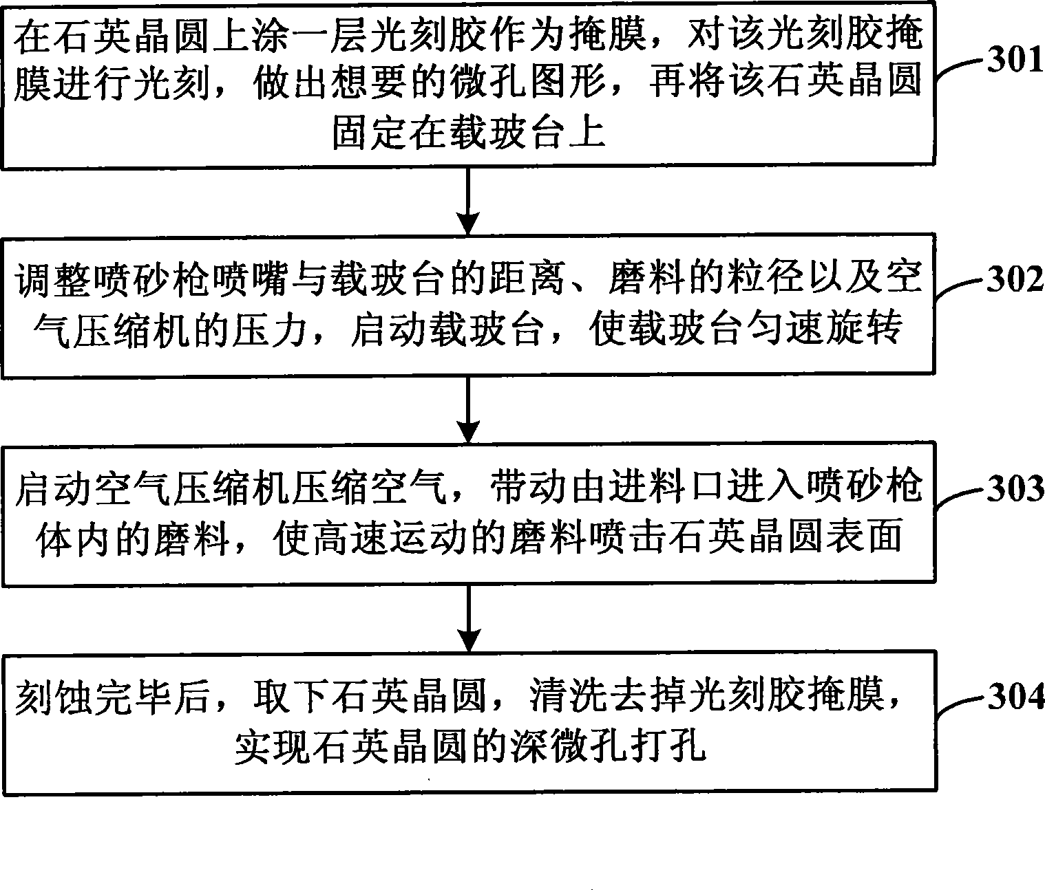
[0038] In order to make the object, technical solution and advantages of the present invention clearer, the present invention will be described in further detail below in conjunction with specific embodiments and with reference to the accompanying drawings.

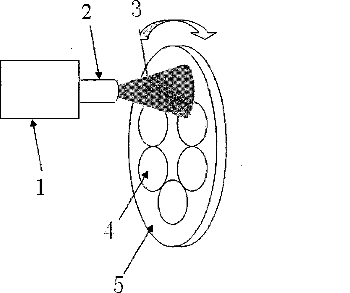
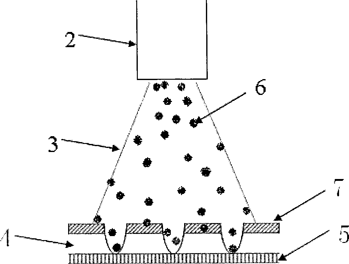
[0039] Such as figure 1 as shown, figure 1 It is a structural schematic diagram of the quartz wafer deep micro-hole processing equipment provided by the present invention, and the equipment includes an air compressor 1 , a sandblasting gun 2 and a glass stage 5 . The compressor 1 is connected to the sandblasting gun 2, and the compressor 1 delivers high-compressed air to the sandblasting gun 2, so that the abrasive in the sandblasting gun 2 is sprayed at a high speed on the quartz wafer placed on the glass stage 5, and the The high-speed moving abrasive hits the quartz material to achieve deep micro-hole processing on the quartz wafer.

[0040] The glass stage 5 is vertically placed and rotated at a constant speed when ...


PUM


Abstract

The invention discloses a device for machining quartz-wafer round deep micropores. The device comprises an air compressor, a sand blasting gun and a glass loading table, wherein the compressor is connected with the sand blasting gun, and the compressor conveys high-compression air to the sand blasting gun, so that abrasive in the sand blasting gun is spouted onto a quartz wafer placed on the glass loading table at a high speed; and a deep micropore is machined on the quartz wafer by utilizing the abrasive in high-speed movement to impact quartz material. The invention simultaneously discloses a deep-micropore machining method for the quartz wafer. By utilizing the invention, the disadvantage that laser can not perforate transparent materials, as well as a series of problems of ion perforation charge, incapability of machining deep micropores and the like, is solved, and deep micropore manufacture on quartz is realized. The device has the advantages of simplicity, implementation easiness, low cost, high etching speed and capability of batch production.

Description

technical field [0001] The invention relates to the technical field of microelectromechanical system (MEMS) microprocessing in microelectronic technology, in particular to the technical field of deep microhole processing of quartz wafers, in particular to a deep microhole processing equipment and method for quartz wafers. Background technique [0002] In the microfabrication of microelectromechanical systems (MEMS), a large number of micropores need to be fabricated, and there are chemical methods and physical methods to realize micropore fabrication. The most common methods of fabricating micropores on substrates are etching, laser drilling, ultrasonic drilling, and ion drilling. [0003] However, the excellent characteristics of quartz make it more and more widely used in the manufacture of MEMS. Due to the selectivity of the etching method, it is impossible to etch microholes on quartz, and because of the light transmission, it is not suitable for laser drilling. It is a...

Claims


Application Information

Patent Timeline
Patent Type & Authority Applications(China)
IPC IPC(8): B81C5/00G03F7/20B81C99/00
Inventor 罗小光刘茂哲李全宝高超群景玉鹏
Owner INST OF MICROELECTRONICS CHINESE ACAD OF SCI
Why Eureka
Try Eureka