Plating apparatus and plating method

A technology of electroplating device and electroplating solution, which is applied in the directions of current conduction device, current insulation device, circuit, etc., can solve the problem of inability to form top-shaped bumps and the like

Active Publication Date: 2009-06-10
EBARA CORP
View PDF3 Cites 33 Cited by
  • Summary
  • Abstract
  • Description
  • Claims
  • Application Information

AI Technical Summary

Problems solved by technology

However, even when electroplating is performed while moving a pair of stirring rods at such a speed, bumps with flat tip shapes cannot be formed.

Method used


Image

  • Plating apparatus and plating method
  • Plating apparatus and plating method
  • Plating apparatus and plating method

Examples


Embodiment Construction

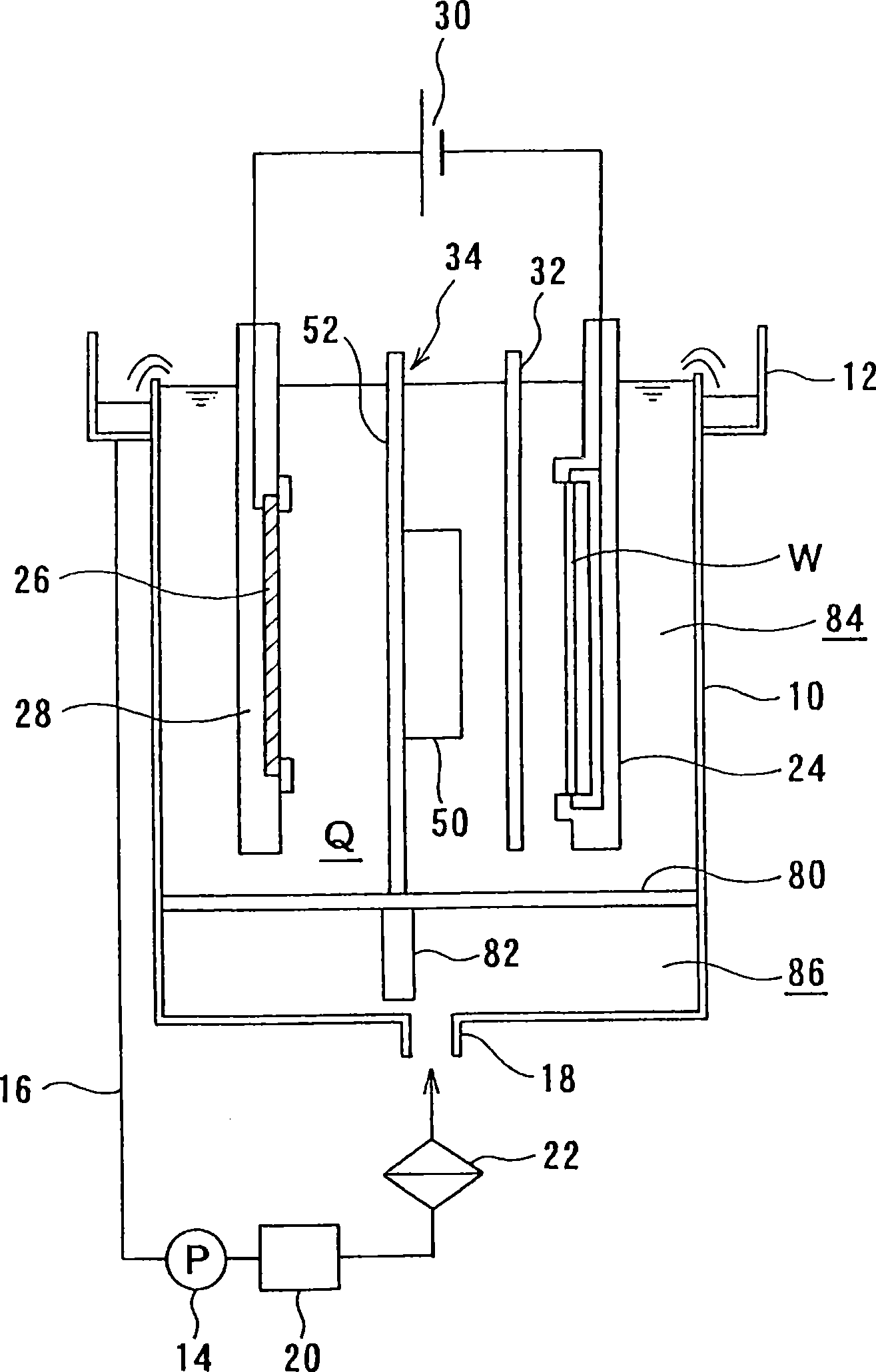
[0103] Embodiments of the present invention will be described below with reference to the drawings. In addition, in the following examples, an example in which copper plating is performed on the surface of a substrate as an object to be plated will be described. In each of the following embodiments, the same or corresponding components are denoted by the same reference numerals, and overlapping descriptions are omitted.

[0104] figure 1 It is a longitudinal sectional front view showing an electroplating apparatus according to an embodiment of the present invention. Such as figure 1 As shown, the electroplating device has an electroplating tank 10 that keeps the electroplating solution Q inside, and on the outer periphery above the electroplating tank 10 , there is an overflow tank 12 that catches the electroplating solution Q overflowing from the edge of the electroplating tank 10 . One end of an electroplating solution supply channel 16 having a pump 14 is connected to th...


PUM

PropertyMeasurementUnit
thicknessaaaaaaaaaa

Abstract

A plating apparatus can form a bump having a flat top or can form a metal film having a good in-plane uniformity even when the plating of a plating object (substrate) is carried out under high-current density conditions. The plating apparatus includes a plating tank for holding a plating solution; an anode to be immersed in the plating solution in the plating tank; a holder for holding a plating object and disposing the plating object at a position opposite the anode; a paddle, disposed between the anode and the plating object held by the holder, which reciprocates parallel to the plating object to stir the plating solution; and a control section for controlling a paddle drive section which drives the paddle. The control section controls the paddle drive section so that the paddle moves at a velocity whose average absolute value is 70 cm/sec to 100 cm/sec.

Description

technical field [0001] The present invention relates to an electroplating device and an electroplating method for electroplating the surface of an object to be electroplated (substrate) such as a semiconductor wafer; in particular, it relates to forming a coating film suitable for fine wiring grooves or holes and protective layer openings provided on the surface of a semiconductor wafer, or A plating apparatus and plating method for forming bumps (bump-shaped electrodes) electrically connected to package electrodes and the like on the surface of a semiconductor wafer. Background technique [0002] For example, in TAB (Tape Automated Bonding) or flip-chip, it is currently being widely implemented to form gold, copper, solder, nickel or more of these materials at predetermined places (electrodes) on the surface of the semiconductor chip on which wiring is formed. The protruding connection electrodes (bumps) stacked in layers are electrically connected to the packaging electrod...

Claims


Application Information

Patent Timeline
Patent Type & Authority Applications(China)
IPC IPC(8): C25D17/00C25D19/00
CPCH01L2924/0002C25D7/12C25D17/001C25D17/08H01L2924/00C25D17/007C25D17/008C25D21/10C25D21/12
Inventor 斋藤信利藤方淳平山本忠明上村健司
Owner EBARA CORP
Why Eureka
Try Eureka