Dry etching apparatus and dry etching method

A dry etching, etching gas technology, applied in coatings, electrical components, circuits, etc., can solve problems such as insufficient etching speed, and achieve the effect of high etching speed and good in-plane uniformity

Active Publication Date: 2010-03-24
ULVAC INC
View PDF4 Cites 1 Cited by
  • Summary
  • Abstract
  • Description
  • Claims
  • Application Information

AI Technical Summary

Problems solved by technology

[0005] However, in the above-mentioned dry etching apparatus, the in-plane uniformity is 10% or more, and there is also a problem that the etching rate is insufficient.

Method used


Image

  • Dry etching apparatus and dry etching method

Examples


Embodiment 1

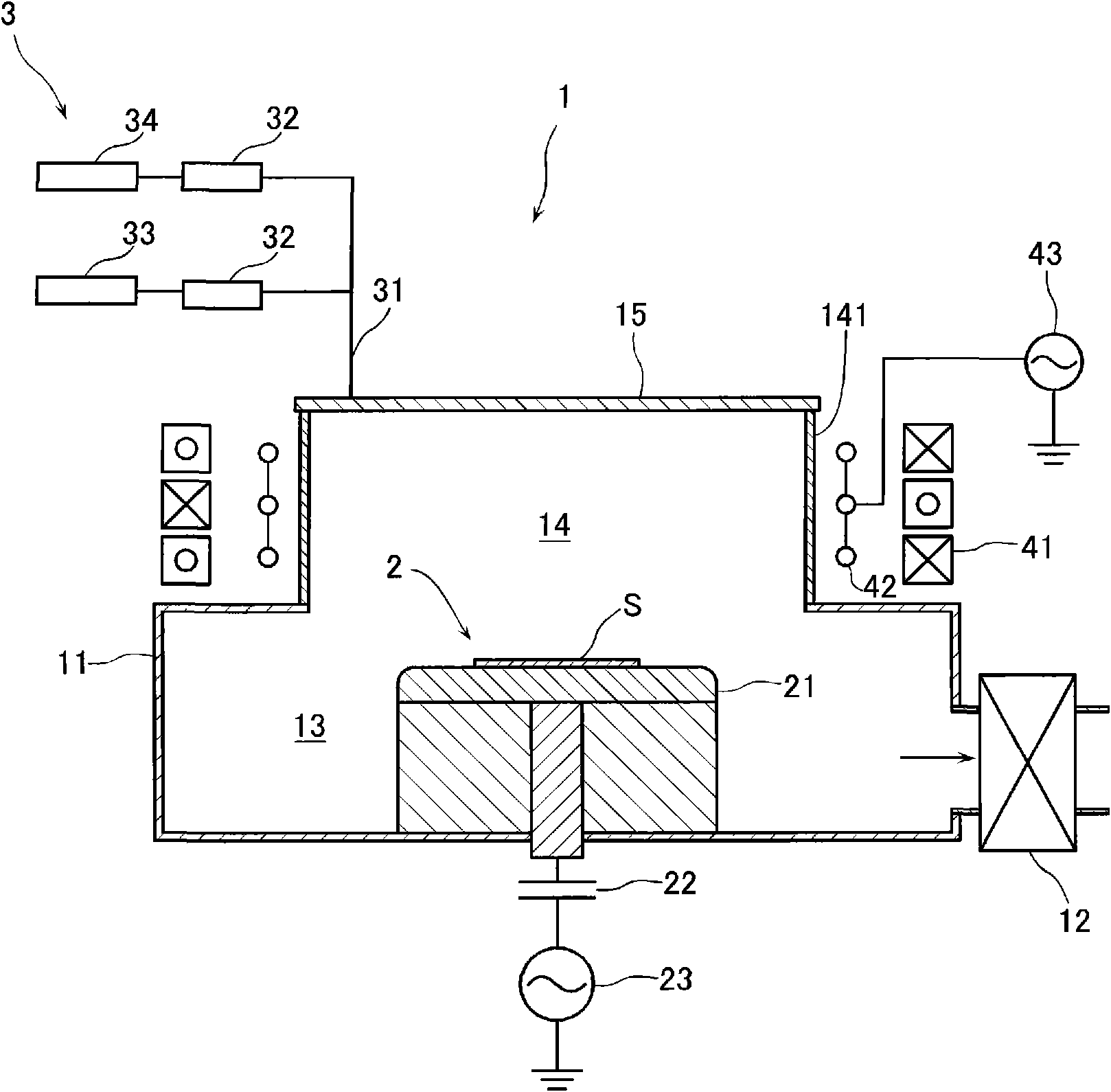
[0039] In this example, use figure 1 The etching device 1 shown performs etching. As the side wall 141, a product named SAPPHAL / Tokyo Ceramics Co., Ltd. was used as the translucent alumina ceramic (specific permittivity: 10, dielectric loss: 1×10 -4 ) to make.

[0040] First, on the substrate mounting table 2 of the etching device 1 in which the side wall 141 of the plasma generation chamber 14 is made of high-purity translucent alumina, a SiO substrate having a thickness of 1 μm is placed. 2 The substrate S to be processed, which is thin film and made of Si, generates plasma by the second high-frequency power supply 43, and at the same time introduces 3 f 8 The etching gas of gas 8 sccm and Ar gas 152 sccm etch the substrate S to be processed. The etching conditions were 400 W for the first high-frequency power supply (substrate side), 1200 W for the second high-frequency power supply (antenna side), set substrate temperature: -20° C., and pressure: 0.6 Pa.

[0041] Afte...

Embodiment 2

[0045] In this example, the difference from Example 1 is that a G-line resist layer was formed with a thickness of 2 μm as the resist layer, and etching was performed under exactly the same conditions except that. The substrate S to be processed was taken out from the etching apparatus 1, and the in-plane uniformity was examined, and the result was plus or minus 9.58%. In addition, the etching rate was 79.5 nm / min.

Embodiment 3

[0050] In this example, the difference from Example 1 is that the Si substrate was used as a sapphire substrate, and etching was performed under exactly the same conditions except that. The substrate S to be processed was taken out from the etching apparatus 1, and the in-plane uniformity was examined, and the result was plus or minus 5%. In addition, the etching rate was 350 nm / min.


PUM

PropertyMeasurementUnit
thicknessaaaaaaaaaa
dielectric lossaaaaaaaaaa

Abstract

A dry etching apparatus having excellent in-plane uniformity and a high etching rate and a dry etching method are provided. A dry etching apparatus includes a vacuum chamber having an upper plasma generation chamber and a lower substrate processing chamber; a magnetic field coil disposed outside a sidewall of the plasma generation chamber; an antenna coil disposed between the magnetic field coil and the outside of the sidewall and connected to a high-frequency power source; and means for introducing an etching gas disposed on top of the plasma generation chamber, wherein the sidewall is formed of a material having a relative dielectric constant of 4 or more.

Description

technical field [0001] The invention relates to a dry etching device and a dry etching method. Background technique [0002] Previously, on SiO covered with a resist mask 2 In the case of etching the interlayer insulating film, the following inductively coupled dry etching method is used, that is, the electrons are accelerated by the induced electric field generated by the high-frequency induced magnetic field, and the etching is performed in the plasma atmosphere generated thereby, and the wiring is etched. Through holes and slots for micro machining. [0003] As an apparatus for implementing such a dry etching method, an inductively coupled dry etching apparatus is known (for example, refer to Patent Document 1). [0004] Patent Document 1: Japanese Unexamined Patent Publication No. 2001-23961 (Claim 1 and figure 1 ) [0005] However, in the above-mentioned dry etching apparatus, the in-plane uniformity is 10% or more, and there is also a problem that the etching rate ...

Claims


Application Information

Patent Timeline
Patent Type & Authority Applications(China)
IPC IPC(8): H01L21/3065C23C4/10
CPCH01J37/16C23C4/00H01J37/321H01J37/3266C23C4/105C23C4/11H01L21/3065
Inventor 森川泰宏邹红红林俊雄
Owner ULVAC INC
Why Eureka
Try Eureka